
Page 411 - Op Amps Design, Applications, and Troubleshooting
P. 411
Nonideal DC Characteristics 387
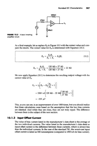
FIGURE 10.3 A basic inverting "=£"
amplifier circuit.
As a final example, let us replace R B in Figure 10.3 with the correct value and com-
pare the results. The correct value for R B is determined with Equation (10.2),
We now apply Equation (10.1) to determine the resulting output voltage with the
correct value of R B.
This, as you can see, is an improvement of over 1000 times, but you should realize
that these calculations were based on the assumption that the two bias currents
are identical. And while they are close, they are not truly equal. The difference
between them is the subject of the next section.
10.1.2 Input Offset Current
The value of bias current listed in the manufacturer's data sheet is the average of
the two individual currents. The value listed in the manufacturer's data sheet as
input offset current is the difference between those currents, which is always less
than the individual currents. In the case of the standard 741, the worst-case input
offset current is listed as 500 nanoamperes (compared to 1500 nA for bias current).