
Page 75 - Op Amps Design, Applications, and Troubleshooting
P. 75
58 AMPLIFIERS
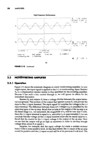
FIGURE 2.10 Continued
2.3 NONINVERTING AMPLIFIER
2.3.1 Operation
Figure 2.11 shows the schematic diagram of a basic noninverting amplifier. As you
might expect, the input signal is applied to the (4-), or noninverting, input. Resistor
R B is a compensation resistor similar to that described for the inverting amplifier.
Because it has such a tiny current through it, we will ignore its effects for the
immediate discussion.
Resistor R F and resistor Rj form a voltage divider between the output termi-
nal and ground. That portion of the output that appears across R/ will provide the
input to the (-) input terminal. The input signal (vj) supplies the voltage to the (+)
input terminal. The difference between these two voltages (%) is amplified by the
open-loop gain of the op amp. Recall that as long as the output of the op amp is in
the linear range (i.e., not saturated), the magnitude of V D will be very near 0 volts.
Since the (+) input terminal is equal to v lt and since V D is approximately 0, we can
conclude that the voltage on the (-) input terminal must also be nearly equal to vj.
Recall that the source for the (-) input voltage is the output of the op amp. Now
we see that the output will go as high as necessary in order to develop enough
voltage drop across R/ to equal u/.
Suppose, for example, that the input voltage (i?/) made a sudden increase
from 0 volts to some positive level. At this first instant, the (+) input of the op amp
would be positive and the (-) input would still be at its previous 0-volt level. The