Page 276 - Optical Communications Essentials
P. 276
Optical Link Design


          266  Chapter Sixteen


                       described by Poole and Nagel, to avoid having a power penalty of 1dB or
                       greater for a fractional time of 30min/yr, the average differential time delay
                       between the two different polarization states must be less than 0.14 of the bit
                       period.
                      ■ The extinction ratio in a laser is defined as the ratio of the “on” power for a
                       logic 1 to the “off” power for a logic 0. (Note that sometimes in earlier litera-
                       ture the extinction ratio is defined alternatively as the ratio of the “off” power
                       for a logic 0 to the “on” power for a logic 1.) Ideally one would like the extinc-
                       tion ratio to be infinite, so that there would be no power penalty from this con-
                       dition. However, the extinction ratio must be finite in an actual system in
                       order to reduce the rise time of laser pulses. The power penalty increases sig-
                       nificantly for lower extinction ratios. If r e represents the ratio of the average
                       power in a logic 1 to the average power in a logic 0, then the power penalty
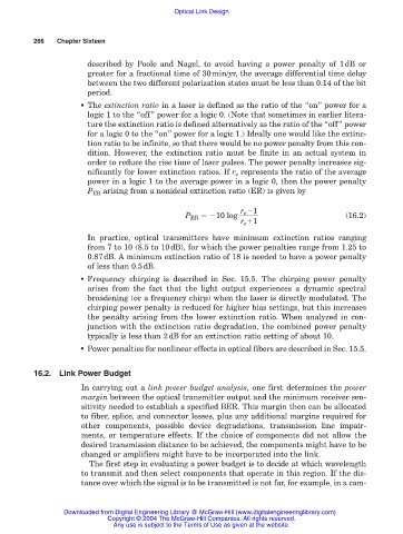
                       P ER arising from a nonideal extinction ratio (ER) is given by

                                                              r e  1
                                                P ER   10 log                           (16.2)
                                                              r e  1
                       In practice, optical transmitters have minimum extinction ratios ranging
                       from 7 to 10 (8.5 to 10dB), for which the power penalties range from 1.25 to
                       0.87dB. A minimum extinction ratio of 18 is needed to have a power penalty
                       of less than 0.5dB.
                      ■ Frequency chirping is described in Sec. 15.5. The chirping power penalty
                       arises from the fact that the light output experiences a dynamic spectral
                       broadening (or a frequency chirp) when the laser is directly modulated. The
                       chirping power penalty is reduced for higher bias settings, but this increases
                       the penalty arising from the lower extinction ratio. When analyzed in con-
                       junction with the extinction ratio degradation, the combined power penalty
                       typically is less than 2dB for an extinction ratio setting of about 10.
                      ■ Power penalties for nonlinear effects in optical fibers are described in Sec. 15.5.


          16.2. Link Power Budget
                      In carrying out a link power budget analysis, one first determines the power
                      margin between the optical transmitter output and the minimum receiver sen-
                      sitivity needed to establish a specified BER. This margin then can be allocated
                      to fiber, splice, and connector losses, plus any additional margins required for
                      other components, possible device degradations, transmission line impair-
                      ments, or temperature effects. If the choice of components did not allow the
                      desired transmission distance to be achieved, the components might have to be
                      changed or amplifiers might have to be incorporated into the link.
                        The first step in evaluating a power budget is to decide at which wavelength
                      to transmit and then select components that operate in this region. If the dis-
                      tance over which the signal is to be transmitted is not far, for example, in a cam-


                 Downloaded from Digital Engineering Library @ McGraw-Hill (www.digitalengineeringlibrary.com)
                            Copyright © 2004 The McGraw-Hill Companies. All rights reserved.
                              Any use is subject to the Terms of Use as given at the website.

