
Page 167 - Organic Electronics in Sensors and Biotechnology
P. 167
144 Cha pte r F o u r
1E–7 0.1
Pyroelectric current response (A) 1E–8 0.01 Pyroelectric voltage response (V)
1E–3
1E–4
1E–9
10 0 10 1 10 2 10 3 10 4
Frequency (Hz)
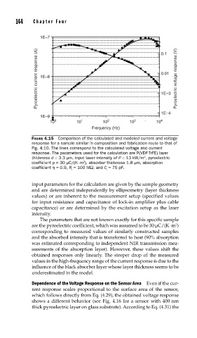
FIGURE 4.15 Comparison of the calculated and modeled current and voltage
response for a sample similar in composition and fabrication route to that of
Fig. 4.10. The lines correspond to the calculated voltage and current
response. The parameters used for the calculation are P(VDF-TrFE) layer
2
thickness d = 3.3 μm, input laser intensity of P = 13 kW/m , pyroelectric
2
coeffi cient p = 30 μC/(K ⋅ m ), absorber thickness 1.8 μm, absorption
coeffi cient η = 0.9, R = 100 MΩ, and C = 75 pF.
i i
input parameters for the calculation are given by the sample geometry
and are determined independently by ellipsometry (layer thickness
values) or are inherent to the measurement setup (specified values
for input resistance and capacitance of lock-in amplifier plus cable
capacitance) or are determined by the excitation setup as the laser
intensity.
The parameters that are not known exactly for this specific sample
2
are the pyroelectric coefficient, which was assumed to be 30 μC/(K ⋅ m )
corresponding to measured values of similarly constructed samples
and the absorbed intensity that is transferred to heat (90% absorption
was estimated corresponding to independent NIR transmission mea-
surements of the absorption layer). However, these values shift the
obtained responses only linearly. The steeper drop of the measured
values in the high-frequency range of the current response is due to the
influence of the black absorber layer whose layer thickness seems to be
underestimated in the model.
Dependence of the Voltage Response on the Sensor Area Even if the cur-
rent response scales proportional to the surface area of the sensor,
which follows directly from Eq. (4.29), the obtained voltage response
shows a different behavior (see Fig. 4.16 for a sensor with 400 nm
thick pyroelectric layer on glass substrate). According to Eq. (4.31) the