
Page 312 - Organic Electronics in Sensors and Biotechnology
P. 312
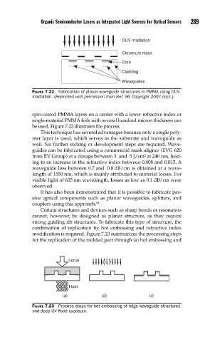
Organic Semiconductor Lasers as Integrated Light Sources for Optical Sensors   289


                                                  DUV irradiation

                                                  Chromium mask
                                                  Core

                                                  Cladding
                                                  Waveguides
               FIGURE 7.22  Fabrication of planar waveguide structures in PMMA using DUV
               irradiation. (Reprinted with permission from Ref. 96. Copyright 2007 IEEE.)


               spin-coated PMMA layers on a carrier with a lower refractive index or
               single-material PMMA foils with several hundred micron thickness can
               be used. Figure 7.22 illustrates the process.
                   This technique has several advantages because only a single poly-
               mer layer is used, which serves as the substrate and waveguide as
               well. No further etching or development steps are required. Wave-
               guides can be fabricated using a commercial mask aligner (EVG 620
               from EV Group) at a dosage between 3  and  5 J/cm² at 240 nm, lead-
               ing to an increase in the refractive index between 0.008 and 0.015. A
               waveguide loss between 0.7 and  0.8 dB/cm is obtained at a wave-
               length of 1550 nm, which is mainly attributed to material losses. For
               visible light of 635 nm wavelength, losses as low as 0.1 dB/cm were
               observed.
                   It has also been demonstrated that it is possible to fabricate pas-
               sive optical components such as planar waveguides, splitters, and
               couplers using this approach. 94
                   Certain structures and devices such as sharp bends or resonators
               cannot, however, be designed as planar structure, as they require
               strong guiding rib structures. To fabricate this type of structure, the
               combination of replication by hot embossing and refractive index
               modification is required. Figure 7.23 summarizes the processing steps
               for the replication of the molded part through (a) hot embossing and


                             Force
                                           DUV


                              Heat

                           (a)            (b)               (c)
               FIGURE 7.23  Process steps for hot embossing of ridge waveguide structures
               and deep UV fl ood exposure.