
Page 314 - Organic Electronics in Sensors and Biotechnology
P. 314
Organic Semiconductor Lasers as Integrated Light Sources for Optical Sensors 291
multiple shims can be electroplated which are good for a couple
thousand embossing cycles. After hot embossing, waveguides are
defined by deep UV exposure of the PMMA substrate. The PMMA
substrate is split into sections by a wafer saw. This sawing process
creates sample end facets of optical quality. However, the substrate is
not completely cut to allow further processing on wafer scale. Subse-
quently, the active laser material Alq :DCM is evaporated through
3
1 mm² wide holes of a high-grade steel mask only onto resonators
(thickness: 180 μm). 97
The demonstrated waveguide-coupled organic semiconductor
lasers uses first-order resonators with a period of 200 nm. The wave-
guides extend over the whole sample width of 25 mm and pass the
resonator fields. The organic lasers are pumped with an elliptical
2
excitation spot with a spot size of 500 × 50 μm .
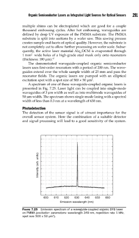
A spectrum of one of these waveguide-coupled organic lasers is
presented in Fig. 7.25. Laser light can be coupled into single-mode
waveguides of 3 μm width as well as into multimode waveguides of
50 μm width. The spectrum shows single-mode lasing with a spectral
width of less than 0.3 nm at a wavelength of 630 nm.
Photodetection
The detection of the sensor signal is of utmost importance for the
overall sensor system. Here the combination of a suitable detector
and signal processing will lead to a good sensitivity of the system.
Intensity (arb. units)
600 610 620 630 640 650 660
Emission wavelength (nm)
FIGURE 7.25 Emission spectrum of a waveguide-coupled organic DFB laser
on PMMA (excitation parameters: wavelength 349 nm, repetition rate 1 kHz,
spot size 500 x 50 μm ).
2