
Page 310 - Organic Electronics in Sensors and Biotechnology
P. 310
Organic Semiconductor Lasers as Integrated Light Sources for Optical Sensors 287
Pump
Microfluidic
diode channel
Organic Organic
lasers photodiode
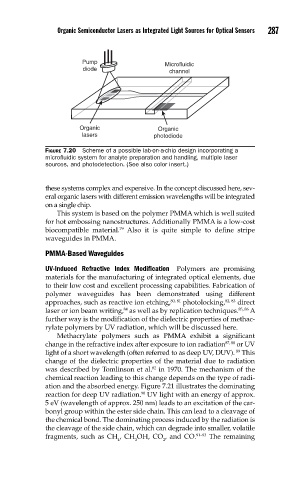
FIGURE 7.20 Scheme of a possible lab-on-a-chip design incorporating a
microfl uidic system for analyte preparation and handling, multiple laser
sources, and photodetection. (See also color insert.)
these systems complex and expensive. In the concept discussed here, sev-
eral organic lasers with different emission wavelengths will be integrated
on a single chip.
This system is based on the polymer PMMA which is well suited
for hot embossing nanostructures. Additionally PMMA is a low-cost
biocompatible material. Also it is quite simple to define stripe
79
waveguides in PMMA.
PMMA-Based Waveguides
UV-Induced Refractive Index Modification Polymers are promising
materials for the manufacturing of integrated optical elements, due
to their low cost and excellent processing capabilities. Fabrication of
polymer waveguides has been demonstrated using different
approaches, such as reactive ion etching, 80, 81 photolocking, 82, 83 direct
laser or ion beam writing, as well as by replication techniques. 85, 86 A
84
further way is the modification of the dielectric properties of methac-
rylate polymers by UV radiation, which will be discussed here.
Methacrylate polymers such as PMMA exhibit a significant
change in the refractive index after exposure to ion radiation 87, 88 or UV
89
light of a short wavelength (often referred to as deep UV, DUV). This
change of the dielectric properties of the material due to radiation
was described by Tomlinson et al. in 1970. The mechanism of the
82
chemical reaction leading to this change depends on the type of radi-
ation and the absorbed energy. Figure 7.21 illustrates the dominating
90
reaction for deep UV radiation. UV light with an energy of approx.
5 eV (wavelength of approx. 250 nm) leads to an excitation of the car-
bonyl group within the ester side chain. This can lead to a cleavage of
the chemical bond. The dominating process induced by the radiation is
the cleavage of the side chain, which can degrade into smaller, volatile
fragments, such as CH , CH OH, CO , and CO. 91–93 The remaining
4 3 2