
Page 89 - PDA Robotics Using Your Personal Digital Assistant to Control Your Robot
P. 89
PDA 05 5/30/03 11:35 AM Page 65
Chapter 5 / The Electronics
Demodulation
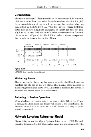
The modulated signal (data) from the IR transceiver module (on RXIR
pin) needs to be demodulated to form the received data (on RX pin).
Once demodulation of the data byte occurs, the received data are
transmitted by the MCP2150 UART (on the RX pin). Figure 5.23 illus-
trates the data decoding. Note: The signal on the RX pin does not actu-
ally line up in time with the bit value that was received on the RXIR
pin, as shown in Figure 5.23. The RXIR bit value is shown to represent
the value to be transmitted on the RX pin.
Figure 5.23
MCP2150 data encoding (demodulated).
Minimizing Power
The device can be placed in a low-power mode by disabling the device
(holding the EN pin at the low state). The internal state machine is
monitoring this pin for a low level. Once this is detected, the device is
disabled and enters into a low-power state.
Returning to Device Operation
When disabled, the device is in a low-power state. When the EN pin
is brought to a high level, the device will return to the operating mode.
The device requires a delay of 1024 TOSC before data may be trans-
mitted or received.
Network Layering Reference Model
Figure 5.24 shows the Open Systems Interconnect (OSI) Network
Layering Reference Model. The shaded areas are implemented by the
65