
Page 85 - PDA Robotics Using Your Personal Digital Assistant to Control Your Robot
P. 85
PDA 05 5/30/03 11:35 AM Page 61
Chapter 5 / The Electronics
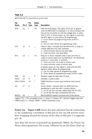
Table 5.2
MCP2150 DIP Pin Descriptions (continued)
Pin Pin Buffer
Name Pin # Type Type Description
DTR 11 I TTL Data Terminal Ready. The value of this pin is ignored
once the MCP2150 is initialized. It is recommended that
this pin be connected so that the voltage level is either
VSS or VCC. At device power up, this signal is used with
the RTS signal to enter device ID programming.
1 = Enter Device ID programming mode (if RTS is
cleared).
0 = Do not enter Device ID programming mode.
CTS 12 O _ Clear to Send. Indicates that the MCP2150 is ready to
receive data from the host controller.
1 = Host controller should not send data.
0 = Host controller may send data.
RTS 13 I TTL Request to Send. Indicates that a host controller is
ready to receive data from the MCP2150. The MCP2150
prepares to send data, if available.
1 = Host controller not ready to receive data.
0 = Host controller ready to receive data.
At device power up, this signal is used with the DTR
signal to enter device ID programming.
1 = Do not enter device ID programming mode.
0 = Enter device ID programming mode (if DTR is set).
VDD 14 _ P Positive supply for logic and I/O pins.
OSC2 15 O _ Oscillator crystal output.
OSC1/CLKIN 16 I CMOS Oscillator crystal input/external clock source
input.
CD 17 O _ Carrier Detect. Indicates that the MCP2150 has
established a valid link with a primary device.
1 = An IR link has not been established (No IR Link).
0 = An IR link has been established (IR Link).
BAUD1 18 I ST BAUD1:BAUD0 specify the baud rate of the device.
Legend: TTL = TTL compatible input; I = Input; P = Power; ST = Schmitt Trigger input with
CMOS levels; O = Output; CMOS = CMOS compatible input
Power Up. Figure 5.20b shows the pin’s physical layout conforming
to the numbering convention of first pin to the top left and the num-
bers wrapping around the bottom of the chip so that pin 1 is opposite
pin 18.
Any time the device is powered up (parameter D003), the Power Up
Timer delay (parameter 33) occurs, followed by an Oscillator Start-up
61