Page 126 - Phase-Locked Loops Design, Simulation, and Applications
P. 126

MIXED-SIGNAL PLL ANALYSIS   Ronald E. Best                                              81


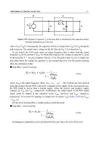
                      Figure 3.19 Charging of capacitor C  in the loop filter is calculated by this equivalent model.
                                                      1
                              Detailed explanations are in the text.
             value of u  is U /2. Consequently, the capacitor will try to charge from U /2 to U  during the
                                                                                            B
                      f
                                                                                    B
                            B
             pull-in process. The actual source voltage for the RC filter in Fig. 3.19 is therefore U .
                                                                                              B
               To get locked, the VCO must create an output frequency that  is offset from the center
             frequency ω  by the amount N Δω . To obtain that frequency the voltage on capacitor C  must
                                                                                                 1
                        0
                                              0
             be increased by N · Δω /K  [compare with Eq. (3.4)]. The pull-in time T  now is simply the
                                     0  0                                            P
             time after which the voltage on capacitor C  has reached that level. For the passive lead-lag
                                                        1
             filter, the calculation yields
             ■ loop filter = passive lead-lag

                                                                                         (3.83)


             where Δω  is the initial frequency offset, Δω  = ω  − ω ′. This formula has been derived
                                                         0
                                                               1
                                                                     0
                      0
             under the premise that the PFD is driven by a unipolar power supply. In the most general case,
             the PFD could be driven from a bipolar supply, where the  positive and negative supply
             voltages are  U  and  U B− , respectively. Furthermore, the output signal of the PFD output
                           B+
             signal could be clipped at the saturation levels  U       (positive) and  U     (negative),
                                                                  sat+                  sat−
             respectively. To account for clipping, we simply have to replace U /2 in Eq. (3.83) by (U sat+
                                                                              B
             − U    )/2.
                sat−
               For the active lead-lag filter, a similar analysis yields the result
             ■ loop filter = active lead-lag


                                                                                         (3.84)


               An analogous computation can be performed for the case where the active PI is used:
   121   122   123   124   125   126   127   128   129   130   131