
Page 274 - Phase-Locked Loops Design, Simulation, and Applications
P. 274
MIXED-SIGNAL PLL APPLICATIONS PART 2: FRACTIONAL-N FREQUENCY
SYNTHESIZERS Ronald E. Best 162
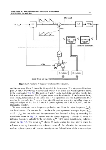
Figure 7.2 A fractional-N frequency synthesizer block diagram.
and the summing block Σ should be disregarded for the moment. The integer and fractional
parts (N and F, respectively) of the division ratio N. F are stored in a buffer register as shown
in the lower part of Fig. 7.2. The numbers N and F can be loaded via a serial or parallel data
link from a microprocessor. The F register stores a fractional number; F can be stored in any
code (binary, hexadecimal, BCD, and so on). If F is represented as a two-digit fractional BCD
number, for example, the F register is an eight-bit register, where the individual states are
assigned weights of 0.8, 0.4, 0.2, and 0.1 (tenths register), and 0.08, 0.04, 0.02, and 0.01
(hundredths register).
We now investigate how a frequency synthesizer can divide its output frequency f by
out
fractional numbers. For example, let’s see how the system generates an output frequency f out
= 5.3 · f . We can understand the operation of the fractional N loop by examining the
ref
waveforms shown in Fig. 7.3. Assume that the output frequency is already 5.3 times the
reference frequency, and refer to the waveforms u ** (VCO output signal) and u (reference
2 1
signal) in Fig. 7.3. The signal u ** shows 53 cycles during the time interval when the
2
reference signal u is executing ten reference cycles. (In the following, the term reference
1
cycle or reference period will be used to designate one full oscillation of the reference signal