
Page 277 - Phase-Locked Loops Design, Simulation, and Applications
P. 277
MIXED-SIGNAL PLL APPLICATIONS PART 2: FRACTIONAL-N FREQUENCY
SYNTHESIZERS Ronald E. Best 164
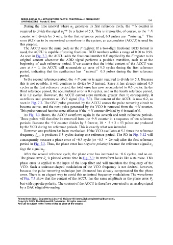
During the time interval where u generates its first reference cycle, the ÷N counter is
1
required to divide the signal u ** by a factor of 5.3. This is impossible, of course, so the ÷N
2
counter will divide by 5 only. In the first reference period, 0.3 pulses are “missing.” This
error (0.3) has to be memorized somewhere in the system; an accumulator (ACCU) is used for
this purpose.
The ACCU uses the same code as the F register. If a two-digit fractional BCD format is
used, the ACCU is capable of storing fractional BCD numbers within a range of 0.00 to 0.99.
As seen in Fig. 7.3, the ACCU adds the fractional number 0.F supplied by the F register to its
original content whenever the ADD signal performs a positive transition, such as at the
beginning of each reference period. If we assume that the initial content of the ACCU was
zero at t = 0, the ACCU will accumulate an error of 0.3 cycles during the first reference
period, indicating that the synthesizer has “missed” 0.3 pulses during the first reference
period.
In the second reference period, the ÷N counter is again required to divide by 5.3. Because
this is not possible, it will continue to divide by 5 instead. Since it has already missed 0.3
cycles in the first reference period, the total error has now accumulated to 0.6 cycles. In the
third reference period, the accumulated error is 0.9 cycles, and in the fourth reference period,
it is 1.2 cycles. However, the ACCU cannot store numbers greater than 1; consequently, it
overflows and generates an OVF signal (Fig. 7.3). The content of the ACCU is now 0.2, as
seen in Fig. 7.3. The OVF pulse generated by the ACCU causes the pulse removing circuit to
become active, and the next pulse generated by the VCO is removed from the ÷N counter.
This pulse removal has the same effect as if the ÷N counter divided by 6 instead of 5.
As Fig. 7.3 shows, the ACCU overflows again in the seventh and tenth reference periods.
Three pulses will therefore be removed from the ÷N counter in a sequence of ten reference
periods. Because the ÷N counter divides by 5 forever, 10 · 5 + 3 = 53 pulses are produced
by the VCO during ten reference periods. This is exactly what was intended.
However, one problem has been overlooked. If the VCO oscillates at 5.3 times the reference
frequency f , it produces 5.3 cycles during one reference period. The PD in Fig. 3.12 will
ref
consequently measure a phase error of −0.3 cycle (or −0.3 · 2π rad) after the first reference
period in Fig. 7.3. Thus, the phase error has negative polarity because the reference signal u 1
lags the signal u .
2
After the second reference cycle, the phase error has increased to −0.6 cycles, and so on.
The phase error θ is plotted versus time in Fig. 7.3; its waveform looks like a staircase. This
e
phase error is applied to the input of the loop filter and will modulate the frequency of the
VCO. Such a staircase-shaped modulation of the VCO frequency is not desired, however,
because the pulse removing technique just discussed has already compensated for the phase
error. There is an elegant way to avoid this undesired frequency modulation: The waveforms
of Fig. 7.3 show that the content of the ACCU has the same amplitude as the phase error θ e
but with opposite polarity. The content of the ACCU is therefore converted to an analog signal
by a DAC (digital-to-analog
Printed from Digital Engineering Library @ McGraw-Hill (www.Digitalengineeringlibrary.com).
Copyright ©2004 The McGraw-Hill Companies. All rights reserved.
Any use is subject to the Terms of Use as given at the website.