
Page 49 - Photodetection and Measurement - Maximizing Performance in Optical Systems
P. 49
Amplified Detection Circuitry
42 Chapter Two
Design for Speed
Signal output falls off Minimize C with:
f
above f = 1/ 2 R C - Chip resistor
π
c
f f
Try transimpedance C f - Compact layout
- SMD opamp
configuration (or compensate)
Focus light if it R f
f
allows a smaller PD I p Use lowest R as long as
V >100mV
o
GBW
C p Reduce effect of R C with fast
f p
amplifier:
Decouple bias BW GBW
π
p
supply at signal Minimize C with: 2 R C
f p
frequencies - Smallest photodiode
- Reverse bias (but watch leakage)
- Low opamp input capacitance
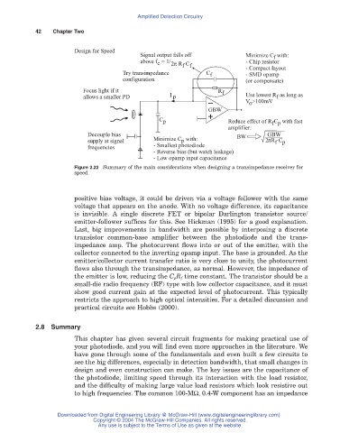
Figure 2.22 Summary of the main considerations when designing a transimpedance receiver for
speed.
positive bias voltage, it could be driven via a voltage follower with the same
voltage that appears on the anode. With no voltage difference, its capacitance
is invisible. A single discrete FET or bipolar Darlington transistor source/
emitter-follower suffices for this. See Hickman (1995) for a good explanation.
Last, big improvements in bandwidth are possible by interposing a discrete
transistor common-base amplifier between the photodiode and the trans-
impedance amp. The photocurrent flows into or out of the emitter, with the
collector connected to the inverting opamp input. The base is grounded. As the
emitter/collector current transfer ratio is very close to unity, the photocurrent
flows also through the transimpedance, as normal. However, the impedance of
the emitter is low, reducing the C p R f time constant. The transistor should be a
small-die radio frequency (RF) type with low collector capacitance, and it must
show good current gain at the expected level of photocurrent. This typically
restricts the approach to high optical intensities. For a detailed discussion and
practical circuits see Hobbs (2000).
2.8 Summary
This chapter has given several circuit fragments for making practical use of
your photodiode, and you will find even more approaches in the literature. We
have gone through some of the fundamentals and even built a few circuits to
see the big differences, especially in detection bandwidth, that small changes in
design and even construction can make. The key issues are the capacitance of
the photodiode, limiting speed through its interaction with the load resistor,
and the difficulty of making large value load resistors which look resistive out
to high frequencies. The common 100-MW, 0.4-W component has an impedance
Downloaded from Digital Engineering Library @ McGraw-Hill (www.digitalengineeringlibrary.com)
Copyright © 2004 The McGraw-Hill Companies. All rights reserved.
Any use is subject to the Terms of Use as given at the website.