
Page 47 - Photodetection and Measurement - Maximizing Performance in Optical Systems
P. 47
Amplified Detection Circuitry
40 Chapter Two
3.0
With RC
2.5
compensation
2.0 No compensation
Voltage (V) 1.5
1.0
0.5
0.0
0 5 10 15 20 25 30 35 40
Time (ms)
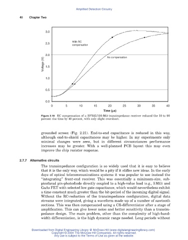
Figure 2.19 RC compensation of a BPX65/100-MW transimpedance receiver reduced the 10 to 90
percent rise time by 40 percent, with only slight overshoot.
grounded screen (Fig. 2.21). End-to-end capacitance is reduced in this way,
although end-to-shield capacitances may be higher. In my experiments only
minimal changes were seen, but in different circumstances performance
increases may be greater. With a well-planned PCB layout this may even
improve the chip resistor response.
2.7.7 Alternative circuits
The transimpedance configuration is so widely used that it is easy to believe
that it is the only way, which would be a pity if it stifles new ideas. In the early
days of optical telecommunications systems it was popular to use instead the
“integrating” front-end receiver. This was essentially a minimum-size, sub-
picofarad pin-photodiode directly coupled to a high-value load (e.g., 5MW) and
GaAs FET with selected low gate capacitance, which would nevertheless exhibit
a time constant much greater than the bit-period of the incoming digital signal.
Without the RC-reduction of the transimpedance configuration, digital data
streams were integrated, giving a waveform made up of a number of sawtooth
sections. This was then compensated using a CR-differentiator after a stage of
amplification. This can give lower noise and better sensitivity than a transim-
pedance design. The main problem, other than the complexity of high-band-
width differentiation, is the high dynamic range needed. Long periods without
Downloaded from Digital Engineering Library @ McGraw-Hill (www.digitalengineeringlibrary.com)
Copyright © 2004 The McGraw-Hill Companies. All rights reserved.
Any use is subject to the Terms of Use as given at the website.