
Page 44 - Photodetection and Measurement - Maximizing Performance in Optical Systems
P. 44
Amplified Detection Circuitry
Amplified Detection Circuitry 37
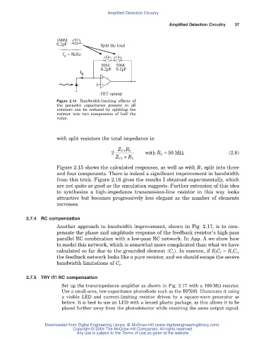
100M
0.2pF Split the load
}
f = 8kHz
c
50M 50M
0.2pF 0.2pF
I p -
+
FET opamp
Figure 2.14 Bandwidth-limiting effects of
the parasitic capacitance present in all
resistors can be reduced by splitting the
resistor into two components of half the
value.
with split resistors the total impedance is:
ZR 2
C
1
2 with R 2 = 50 MW. (2.6)
Z C 1 + R 2
Figure 2.15 shows the calculated responses, as well as with R 1 split into three
and four components. There is indeed a significant improvement in bandwidth
from this trick. Figure 2.16 gives the results I obtained experimentally, which
are not quite as good as the simulation suggests. Further extension of this idea
to synthesize a high-impedance transmission-line resistor in this way looks
attractive but becomes progressively less elegant as the number of elements
increases.
2.7.4 RC compensation
Another approach to bandwidth improvement, shown in Fig. 2.17, is to com-
pensate the phase and amplitude response of the feedback resistor’s high-pass
parallel RC combination with a low-pass RC network. In App. A we show how
to model this network, which is somewhat more complicated than what we have
calculated so far due to the grounded element (C c ). In essence, if R f C f = R c C c ,
the feedback network looks like a pure resistor, and we should escape the severe
bandwidth limitations of C f .
2.7.5 TRY IT! RC compensation
Set up the transimpedance amplifier as shown in Fig. 2.17 with a 100-MW resistor.
Use a small-area, low-capacitance photodiode such as the BPX65. Illuminate it using
a visible LED and current-limiting resistor driven by a square-wave generator as
before. It is best to use an LED with a lensed plastic package, as this allows it to be
placed further away from the photodetector while receiving the same output signal.
Downloaded from Digital Engineering Library @ McGraw-Hill (www.digitalengineeringlibrary.com)
Copyright © 2004 The McGraw-Hill Companies. All rights reserved.
Any use is subject to the Terms of Use as given at the website.