
Page 39 - Photodetection and Measurement - Maximizing Performance in Optical Systems
P. 39
Amplified Detection Circuitry
32 Chapter Two
4.0
3.5
3.0
2.5
Voltage (V) 1.5
2.0
1.0
0.5
0.0
-0.5
-1.0
-250 -200 -150 -100 -50 0 50 100 150 200 250
Time (ms)
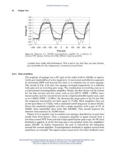
Figure 2.9 Response of a 100-MW transimpedance amplifier for a selection of
common FET opamps, showing the wildly different responses possible.
a couple show really odd performance. This is not to say that they are poor devices,
just unsuitable for the components I connected around them.
2.6.3 Dual amplifiers
The majority of opamps has a DC gain of the order of 80 to 100dB, or equiva-
lently gain bandwidths of a few megahertz. A convenient and effective approach
to increasing GBW well beyond this limit is to combine two or more opamps.
The circuit of Fig. 2.10 uses two opamps arranged respectively as a follower
with gain and an inverting gain stage. The combination is inverting, just as in
a conventional transimpedance amplifier. Ideally, the first device can be chosen
for low bias current and low noise, such as the AD711 (GBW = 4MHz) men-
tioned earlier, and the second device can be a high-bandwidth bipolar unit, such
as an LM833 (GBW = 15MHz). By choosing the stage gains to be 52 and 192,
the respective bandwidths are both equal to 77kHz. Both amplifiers then act
as low-pass filters at 77kHz, with a combined cutoff frequency of about 54kHz.
4
Hence the combined amplifier acts like a single amplifier with a gain of 10 at
54kHz. Gain bandwidth then looks like 540MHz. This should improve the
detector time-constant by 23,000 times.
Figure 2.11 is another way to combine two opamps, described in several data
sheets from Burr-Brown. Here a composite amplifier is again formed from a
low-bias current FET front end and a high-speed bipolar gain stage. No DC local
feedback is applied, so at DC the loop gain is the product of the two amplifiers’
gains (225dB). At higher frequencies, the gain is reduced by the integrator
around the second amplifier. Transimpedance feedback is applied around both
amplifiers, as normally. The signal output is just as for the same feedback resis-
Downloaded from Digital Engineering Library @ McGraw-Hill (www.digitalengineeringlibrary.com)
Copyright © 2004 The McGraw-Hill Companies. All rights reserved.
Any use is subject to the Terms of Use as given at the website.