Page 300 - Power Electronic Control in Electrical Systems
P. 300
//SYS21/F:/PEC/REVISES_10-11-01/075065126-CH007.3D ± 288 ± [263±289/27] 17.11.2001 10:25AM
288 Harmonic studies of power compensating plant
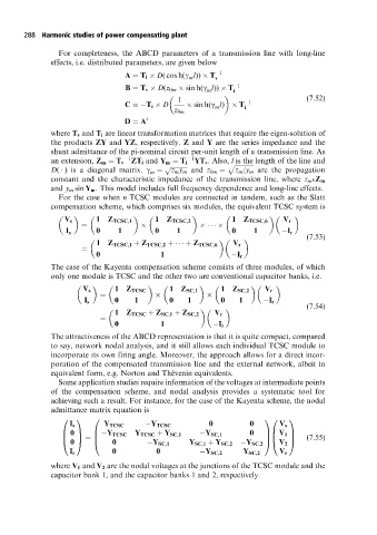
For completeness, the ABCD parameters of a transmission line with long-line
effects, i.e. distributed parameters, are given below
A T i D( cos h(g l)) T 1
m
v
B T v D(z 0m sin h(g l)) T 1
i
m
1 1 (7:52)
C T i D sin h(g l) T i
m
z 0m
D A t
where T v and T i are linear transformation matrices that require the eigen-solution of
the products ZY and YZ, respectively. Z and Y are the series impedance and the
shunt admittance of the pi-nominal circuit per-unit length of a transmission line. As
1 1
an extension, Z m T v ZT i and Y m T i YT v . Also, l is the length of the line and
p p
z m y m and z 0m
D( ) is a diagonal matrix. g z m /y m are the propagation
m
constant and the characteristic impedance of the transmission line, where z m Z m
and y m sin Y m . This model includes full frequency dependence and long-line effects.
For the case when n TCSC modules are connected in tandem, such as the Slatt
compensation scheme, which comprises six modules, the equivalent TCSC system is
V s 1 Z TCSC,1 1 Z TCSC,2 1 Z TCSC,6 V r
I s 0 1 0 1 0 1 I r
(7:53)
1 Z TCSC,1 Z TCSC,2 Z TCSC,6 V r
0 1 I r
The case of the Kayenta compensation scheme consists of three modules, of which
only one module is TCSC and the other two are conventional capacitor banks, i.e.
V s 1 Z TCSC 1 Z SC,1 1 Z SC,2 V r
I s 0 1 0 1 0 1 I r
(7:54)
1 Z TCSC Z SC,1 Z SC,2 V r
0 1 I r
The attractiveness of the ABCD representation is that it is quite compact, compared
to say, network nodal analysis, and it still allows each individual TCSC module to
incorporate its own firing angle. Moreover, the approach allows for a direct incor-
poration of the compensated transmission line and the external network, albeit in
equivalent form, e.g. Norton and The  venin equivalents.
Some application studies require information of the voltages at intermediate points
of the compensation scheme, and nodal analysis provides a systematic tool for
achieving such a result. For instance, for the case of the Kayenta scheme, the nodal
admittance matrix equation is
0 1 0 10 1
I s Y TCSC Y TCSC 0 0 V s
0 0
B C B Y TCSC Y TCSC Y SC,1 Y SC,1 CB V 1 C
B C B CB C (7:55)
0 0
@ A @ Y SC,1 Y SC,1 Y SC,2 Y SC,2 A@ V 2 A
0 0
I r Y SC,2 Y SC,2 V r
where V 1 and V 2 are the nodal voltages at the junctions of the TCSC module and the
capacitor bank 1, and the capacitor banks 1 and 2, respectively.

