
Page 152 - Power Electronics Handbook
P. 152
D.C. link frequency converters 145
so prevent voltage transients during switchsff, which could destroy the
semiconductors. D.C. line control circuits are described further in Chapter
12.
6.7 D.C. link lrequency converters
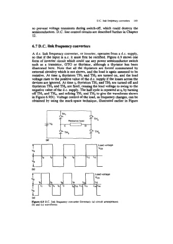
A d.c. link frequency converter, or inverter, operates from a d.c. supply,
so that if the input is 8.c. it must first be rectified. Figure 6.9 shows one
form of inverter circuit which could use any power semiconductor switch
such as a transistor, GTO or thyristor, although a thyristor has been
illustrated here. Note that all the thyristors are forced commutated by
external circuitry which is not shown, and the load is again assumed to be
resistive. At time lo thyristors TH1 and TH2 are turned on, and the load
voltage rises to the positive value of the d.c. supply if the losses across the
devices are ignored. At time r3 thyristors TH1 and TH2 are turned off and
thyristors TH3 and T€& are fired, causing the load voltage to swing to the
negative value of the d.c. supply. The half cycle is repeated at by turning
off TH3 and TH,, and refiring TH1 and TH2 to give the waveforms shown
in Figure 6.9(b). Voltage control of the load, as frequency changes, can be
obtained by using the mark-space technique, illustrated earlier in Figure
voltage
f-Jl!\ tz t4 t5rrlj rntLvoltage
t71
t13
t10
tl6
t14
VB
(Cl
F’igure 6.9 D.C. link frequency converter (inverter): (a) circuit arrangement;
(b) and (c) waveforms