
Page 147 - Power Electronics Handbook
P. 147
140 Power semiconductor circuits - a &sum6
VAS
(d)
(C)
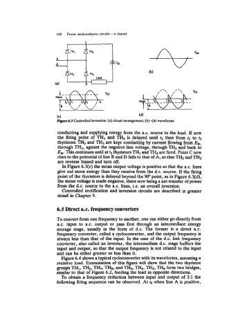
6.3 Controlled inversion: (a) circuit arrangement; (b)-(d) waveforms
conducting and supplying energy from the a.c. source to the load. If now
the firing point of TH1 and TH4 is delayed until r3 then from r2 to 4
thyristors TH2 and TH3 are kept conducting by current flowing from EB,
through TH3, against the negative line voltage, through TH2 and back to
EB. This continues until at f3 thyristors THl and TH4 are fired. Point C now
rises to the potential of line B and D falls to that of A, so that TH2 and TH3
are reverse biased and turn off.
In Figure 6.3(c) the mean output voltage is positive so that the a.c. lines
give out more energy than they receive from the d.c. source. If the firing
point of the thyristors is delayed beyond the 90" point, as in Figure 6.3(d),
the mean voltage is made negative, there now being a net transfer of power
from the d.c. source to the a.c. lines, i.e. an overall inversion.
Controlled rectification and inversion circuits are described in greater
detail in Chapter 9.
6.5 Mrect 8.c. frequency converters
To convert from one frequency to another, one can either go directly from
a.c. input to a.c. output or pass first through an intermediate energy
storage stage, usually in the form of d.c. The former is a direct a.c.
frequency converter, called a cycloconverter, and the output frequency is
always less than that of the input. In the case of the d.c. link frequency
converter, also called an inverter, the intermediate d.c. stage buffers the
input and output, so that the output frequency is not related to the input
and can be either greater or less than it.
Figure 6.4 shows a typical cycloconverter with its waveforms, assuming a
resistive load. Examination of this figure will show that the two thyristor
groups TH1, TH2, TH,, TH8, and TH3, TI-€+, TH5, form two bridges,
similar to that of Figure 6.2, feeding the load in opposite directions.
To obtain a frequency reduction between input and output of 3:l the
foilowing firing sequence can be observed. At to when line A is positive,