
Page 304 - Power Electronics Handbook
P. 304
294 D.C. link frequency changers
collector current waveform now being as in Figure 13.8(b). The frequency
of operation is once again determined by the maximum collector current,
but now the magnetising current builds up rapidly, once transformer
saturation has commenced, and this swamps the variation in load current,
so the operating frequency is less load sensitive.
In the circuit of Figure 13.7 it has been assumed that at switch-on one of
the transistors commences to turn on. This may not be the case, especially
on heavy load currents when the loop gain of the system is below unity, so
that the circuit may fail to oscillate. To prevent this, several starting circuits
are used, Figure 13.9 showing two of the simplest techniques. In the
resistor-starting circuit the resistor chain R1 and Rz provides the initial bias
for turn-on, the transistor with the highest gain turning on first. Thereafter
the circuit performs as before, the starting resistors having very little effect.
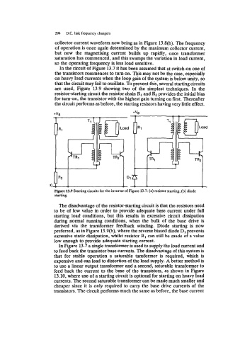
Figure 13.9 Starting circuits for the inverter of Figure 13.7: (a) resistor starting; (b) diode
starting
The disadvantage of the resistor-starting circuit is that the resistors need
to be of low value in order to provide adequate base current under full
starting load conditions, but this results in excessive circuit dissipation
during normal running conditions, when the bulk of the base drive is
derived via the transformer feedback winding. Diode starting is now
preferred, as in Figure 13.9(b), where the reverse biased diode D1 prevents
excessive static dissipation, whilst resistor R1 can still be made of a value
low enough to provide adequate starting current.
In Figure 13.7 a single transformer is used to supply the load current and
to feed back the transistor base currents. The disadvantage of this system is
that for stable operation a saturable tansformer is required, which is
expensive and can lead to distortion of the load supply. A better method is
to use a linear output transformer and a second, saturable transformer to
feed back the current to the base of the transistors, as shown in Figure
13.10, where use of a starting circuit is optional for starting on heavy load
currents. The second saturable transformer can be made much smaller and
cheaper since it is only required to carry the base drive currents of the
transistors. The circuit performs much the same as before, the base current