
Page 307 - Power Electronics Handbook
P. 307
Inverter circuits 297
inverter losses, caused by the circulation of commutation current (for
example, via L1-D1-C-THz) make it inefficient at high frequencies. The
most usual voltage-control system consists of two parallel inverters, with a
common secondary, whose square wave outputs are phase shifted to give a
mark-space controlled voltage output.
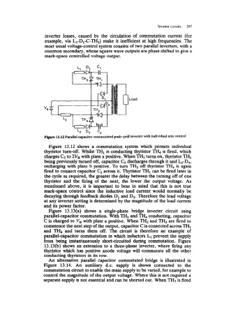
13.12 Parallel capacitor commutated push-pull inverter with individual ann control
Figure 13.12 shows a commutation system which permits individual
thyristor turn-off. Whilst TH1 is conducting thyristor 'Il& is fired, which
charges C, to 2vB with plate a positive. When turns on, thyristor THI
being previously turned off, capacitor C, discharges through it and b-D4,
recharging with plate b positive. To turn THz off thyristor TH, is again
fired to connect capacitor C, across it. Thyristor TH1 can be fired later in
the cycle as required, the greater the delay between the turning off of one
thyristor and the firing of the next, the lower the output voltage. As
mentioned above, it is important to bear in mind that this is not true
mark-space control since the inductive load current would normally be
decaying through feedback diodes D1 and Dz. Therefore the load voltage
at any inverter setting is determined by the magnitude of the load current
and its power factor.
Figure 13.13(a) shows a single-phase bridge inverter circuit using
parallel-capacitor commutation. With TH1 and TI& conducting, capacitor
C is charged to VB with plate a positive. When THz and TH3 are fired to
commence the next step of the output, capacitor C is connected across THI
and TH, and turns them off. The circuit is therefore an example of
parallel-capacitor commutation in which inductors L1 prevent the supply
from being instantaneously short-circuited during commutation. Figure
13.13(b) shows an extension to a three-phase inverter, where firing any
thyristor which has positive anode voltage will commutate all the other
conducting thyristors in its row.
An alternative parallel capacitor commutated bridge is illustrated in
Figure 13.14. An auxiliary d.c. supply is shown connected to the
commutation circuit to enable the main supply to be varied, for example to
control the magnitude of the output voltage. Where this is not required a
separate supply is not essential and can be shorted out. When TH7 is fired