
Page 303 - Power Electronics Handbook
P. 303
Inverter circuits 293
fa)
'L
t2 tg -----f-
(b)
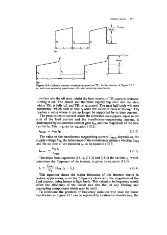
Figure 13.8 Collector current waveform in transistor TR, for the inverter of Figure 13.7:
(a) with non-saturating transformer; (b) with saturating transformer
it further into the off state, whilst the base current to TR2 starts to increase,
turning it on. The circuit will therefore rapidly flip over into the state
where TR1 is fully off and TR2 is saturated. The next half cycle will now
commence, which ends at time t2 when the collector current through TR2
reaches a value where it can no longer be supported by its base current.
The peak collector current which the transistor can support, equal to the
sum of the load current and the transformer-magnetising current, is
determined by its common emitter gain hFE and the magnitude of the base
current t,. This is given by equation (I 3.2).
k(pk) = hFEzB (13.2)
The value of the transformer magnetising current ZmG depends on the
supply voltage VB, the inductance of the transformer primary winding LPm
and the on time of the transistor tc, as in equation (13.3).
(13.3)
Therefore from equations (13.1), (13.2) and (13.3) the on time tc, which
determines the frequency of the inverter, is given by equation (13.4).
(13.4)
This equation shows the major limitation of this inverter circuit in
certain applications, since the frequency vanes with the magnitude of the
load current, being lowest at light loads. This variation in frequency would
affect the efficiency of the circuit and also that of any filtering and
decoupling components which may be used.
To overcome the problem of frequency variation with load the linear
transformer in Figure 13.7 can be replaced by a saturable transformer, the