
Page 298 - Power Electronics Handbook
P. 298
288 D.C. link frequency changers
is impressed across AE and if the two halves of the load are closely coupled
this raises the collector of TR2 to a potential of 2VB above its emitter.
Therefore all the semiconductor devices need to have a voltage rating
equal to at least twice that of the supply.
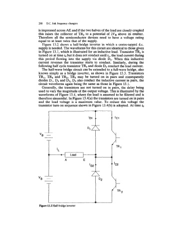
Figure 13.2 shows a half-bridge inverter in which a centre-tapped d.c.
supply is needed. The waveforms for this circuit are identical to those given
in Figure 13.1, which is illustrated for an inductive load. Transistor TRl is
turned on at time to but it does not conduct until tl, the load current during
this period flowing into the supply via diode D1. When this inductive
current reverses the transistor starts to conduct. Similarly, during the
following half cycle transistor TR2 and diode D2 conduct the load current.
The half-wave bridge circuit can be extended to a full-wave bridge, also
known simply as a bridge inverter, as shown in Figure 13.3. Transistors
TR1, T& and TR2, TR3 may be turned on in pairs and consequently
diodes D1, D4 and D2, D3 also conduct the inductive current in pairs, the
circuit waveforms again being the same as those in Figure 13.1.
Generally, the transistors are not turned on in pairs, the delay being
used to vary the magnitude of the output voltage. This is illustrated by the
waveforms of Figure 13.4, where the load is assumed to be filtered and is
therefore sinusoidal. In Figure 13.4(a) the transistors are turned on in pairs
and the load voltage is a maximum value. To reduce this voltage the
transistor turn-on sequence shown in Figure 13.4(b) is adopted. At time to
I i:
VB
Figure 13.2 Half-bridge inverter