
Page 18 - Principles and Applications of NanoMEMS Physics
P. 18
4 Chapter 1
is advised to consult these. The exposition undertaken here is cursory in
nature and only aims at providing an understanding of the fundamentals and
issues of present and future NanoMEMS fabrication technologies.
1.2.1 Conventional IC Fabrication Processes
Conventional IC processes are based on photolithography and chemical
etching, and are synthesized by the iterative application to a wafer of a cyclic
sequence of steps, namely: Spin-casting and patterning, material deposition,
and etching. The salient elements of these steps are presented in what
follows.
1.2.1.1 Spin-Casting
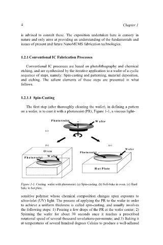
The first step (after thoroughly cleaning the wafer), in defining a pattern
on a wafer, is to coat it with a photoresist (PR), Figure 1-1, a viscous light-
Figure 1-1. Coating wafer with photoresist. (a) Spin-casting. (b) Soft-bake in oven. (c) Hard
bake in hot plate.
sensitive polymer whose chemical composition changes upon exposure to
ultraviolet (UV) light. The process of applying the PR to the wafer in order
to achieve a uniform thickness is called spin-casting, and usually involves
the following steps: 1) Pouring a few drops of the PR at the wafer center; 2)
Spinning the wafer for about 30 seconds once it reaches a prescribed
rotational speed of several thousand revolutions-per-minute; and 3) Baking it
at temperatures of several hundred degrees Celsius to produce a well-adhered