
Page 20 - Principles and Applications of NanoMEMS Physics
P. 20
6 Chapter 1
hardens the PR, whereas in the latter, UV exposure weakens the PR. Thus,
subsequently, when the UV-exposed wafer is etched, the weakened parts of
the PR will be dissolved and the desired pattern revealed. There are two
techniques to dissolve the PR, namely, wet and dry etching. These are
presented next.
1.2.1.2.1 Lithography
The highest resolution (minimum size) and quality of the pattern to be
defined on a wafer depends on how well the mask image is transferred to the
PR. Image formation, in turn, is determined by the lithographic process and
type of PR employed. The lithographic process can make use of an optical
source, an electron beam source, or an X-ray source for creating the desired
pattern on the wafer. In this section we deal with the first and the last
approaches.
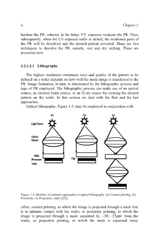
Optical lithography, Figure 1-3, may be employed in conjunction with
(b)
(c)
(a) (a) (b) (c)
Light Source
Light Source
Optical
Optical
System
System
Mask
Mask
Gap
Photoresist Gap
Photoresist
Wafer
Wafer
Figure 1-3. Sketches of common approaches to optical lithography. (a) Contact printing. (b)
Proximity. (c) Projection. (After [23]).
either, contact printing, in which the image is projected through a mask that
is in intimate contact with the wafer, or proximity printing, in which the
image is projected through a mask separated by ~10 − 25 µ m from the
wafer, or projection printing, in which the mask is separated many