
Page 25 - Principles and Applications of NanoMEMS Physics
P. 25
1. NANOELECTROMECHANICAL SYSTEMS 11
(EDP). Detailed experiments to elucidate the mechanism responsible for
anisotropic etching have been undertaken [23]. The fundamental principle
behind anisotropic etching appears to be this: when different crystal planes
possess different atomic densities, those planes with greater density will etch
at a slower rate than those with lower atomic density.
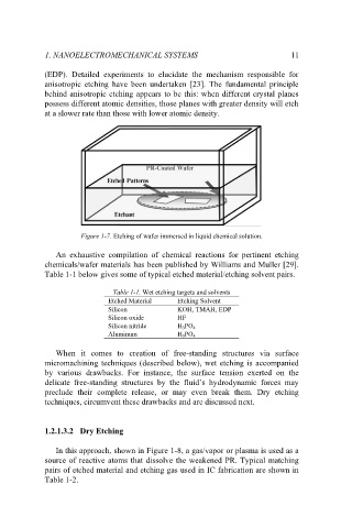
Figure 1-7. Etching of wafer immersed in liquid chemical solution.
An exhaustive compilation of chemical reactions for pertinent etching
chemicals/wafer materials has been published by Williams and Muller [29].
Table 1-1 below gives some of typical etched material/etching solvent pairs.
Table 1-1. Wet etching targets and solvents
Etched Material Etching Solvent
Silicon KOH, TMAH, EDP
Silicon oxide HF
Silicon nitride H 3 PO 4
Aluminum H 3 PO 4
When it comes to creation of free-standing structures via surface
micromachining techniques (described below), wet etching is accompanied
by various drawbacks. For instance, the surface tension exerted on the
delicate free-standing structures by the fluid’s hydrodynamic forces may
preclude their complete release, or may even break them. Dry etching
techniques, circumvent these drawbacks and are discussed next.
1.2.1.3.2 Dry Etching
In this approach, shown in Figure 1-8, a gas/vapor or plasma is used as a
source of reactive atoms that dissolve the weakened PR. Typical matching
pairs of etched material and etching gas used in IC fabrication are shown in
Table 1-2.