
Page 29 - Principles and Applications of NanoMEMS Physics
P. 29
1. NANOELECTROMECHANICAL SYSTEMS 15
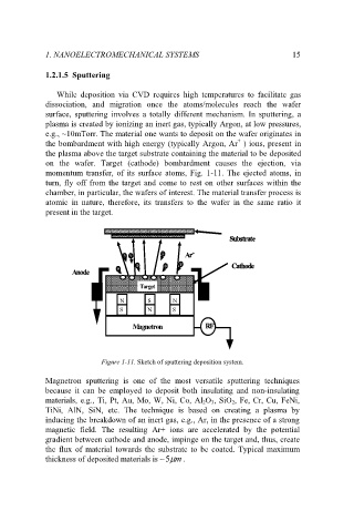
1.2.1.5 Sputtering
While deposition via CVD requires high temperatures to facilitate gas
dissociation, and migration once the atoms/molecules reach the wafer
surface, sputtering involves a totally different mechanism. In sputtering, a
plasma is created by ionizing an inert gas, typically Argon, at low pressures,
e.g., ~10mTorr. The material one wants to deposit on the wafer originates in
+
the bombardment with high energy (typically Argon, Ar ) ions, present in
the plasma above the target substrate containing the material to be deposited
on the wafer. Target (cathode) bombardment causes the ejection, via
momentum transfer, of its surface atoms, Fig. 1-11. The ejected atoms, in
turn, fly off from the target and come to rest on other surfaces within the
chamber, in particular, the wafers of interest. The material transfer process is
atomic in nature, therefore, its transfers to the wafer in the same ratio it
present in the target.
Substrate
Substrate
Ar
Ar + +
Cathode
Cathode
Anode
Anode
Target
Target
N N N N S S S S N N N N
S S S S N N N N S S S S
RF
Magnetron
Magnetron RF
Figure 1-11. Sketch of sputtering deposition system.
Magnetron sputtering is one of the most versatile sputtering techniques
because it can be employed to deposit both insulating and non-insulating
materials, e.g., Ti, Pt, Au, Mo, W, Ni, Co, Al 2O 3, SiO 2, Fe, Cr, Cu, FeNi,
TiNi, AlN, SiN, etc. The technique is based on creating a plasma by
inducing the breakdown of an inert gas, e.g., Ar, in the presence of a strong
magnetic field. The resulting Ar+ ions are accelerated by the potential
gradient between cathode and anode, impinge on the target and, thus, create
the flux of material towards the substrate to be coated. Typical maximum
m
thickness of deposited materials is ~ µ .
5