
Page 28 - Principles and Applications of NanoMEMS Physics
P. 28
14 Chapter 1
Table 1-3. Common CVD reactions and deposition temperatures for
pertinent materials. [24]
Product Reactants Deposition temperature (°C)
Silicon dioxide SiH 4 +CO 2 +H 2 850-950
SiCl 2 H 2 +N 2 O 850-900
SiH 4 +N 2 O 750-850
SiH 4 +NO 650-750
Si(OC 2 H5) 4 650-750
400-450
SiH 4 +O 2
Silicon nitride SiH 4 +NH 3 700-900
650-750
SiCl 2 H 2 +NH 3
Polysilicon SiH 4 600-650
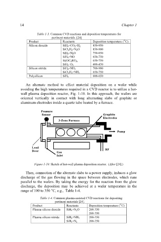
An alternate method to effect material deposition on a wafer while
avoiding the high temperatures required in a CVD reactor is to utilize a hot-
wall plasma deposition reactor, Fig. 1-10. In this approach, the wafers are
oriented vertically in contact with long alternating slabs of graphite or
aluminum electrodes inside a quartz tube heated by a furnace.
Pressure
Pressure
Graphite
Sensor Graphite
Sensor
Electrodes
Electrodes
3-Zone Furnace
3-Zone Furnace
Pump p
Pum
Load
Load
RF
RF
Door
Door
Gas
Gas
Inlet
Inlet
Figure 1-10. Sketch of hot-wall plasma deposition reactor. (After [24].)
Then, connection of the alternate slabs to a power supply, induces a glow
discharge of the gas flowing in the space between electrodes, which runs
parallel to the wafers. By taking the energy for the reaction from the glow
discharge, the deposition may be achieved at a wafer temperature in the
range of 100 to 350 °C, e.g., Table 1-4.
Table 1-4. Common plasma-assisted CVD reactions for depositing
pertinent materials [24].
Product Reactants Deposition temperature (°C)
Plasma silicon dioxide SiH 4 +N 2 O 200-350
200-350
Plasma silicon nitride SiH 4 +NH 3 200-350
200-350
SiH 4 +N 2