
Page 26 - Principles and Applications of NanoMEMS Physics
P. 26
12 Chapter 1
Table 1-2. Etched material-etching gas pairs.
Silicon or Polysilicon SF 6 , CF 4
Silicon dioxide CHF 4 /H 2
Silicon nitride CF4/O2
Aluminum BCl 2
Two fluorine-containing gases have been recently adopted for dry
etching processes, namely, Xenon difluoride, XeF 2 [30] and Boron Fluoride,
BrF 3 [30]. XeF 2 enables an isotropic dry-etch process for silicon, which is
very selective to aluminum, silicon dioxide, silicon nitride and photoresist.
The XeF 2 gas is particularly useful in the post-processing of CMOS ICs. It
can be sublimated from its solid form at 1 Torr and room temperature and,
when applied to solid-phase Si, it obeys the following reaction:
2XeF 2 + SiÆ2Xe+SiF 4
XeF 2 etching of Si achieves high selectivity with a number of masking
materials, such as, SiO 2, Si 3N 4, Al, PR, and phosphosilicate glass (PSG), at
etching rates ranging from 1− 3µ m / min to as high as 40µ m / min [30],
and is characterized by the production of measurable amounts of heat. When
in the presence of water or vapor, XeF 2 reacts with them to form HF. In
terms of its potential application to nanostructure formation, XeF 2 etching
has the drawback that the resulting surfaces tend to have a granular finish
m
10
with a feature size of about µ .
Etch
Etch
Gas
Gas Pump
Pump
Wafers
Wafers
Ground Cathode
Ground
Cathode
Shield
Shield
RF
RF
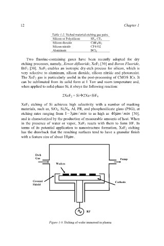
Figure 1-8. Etching of wafer immersed in plasma