
Page 23 - Principles and Applications of NanoMEMS Physics
P. 23
1. NANOELECTROMECHANICAL SYSTEMS 9
the developer from permeating the PR film, no film swelling is produced and
a greater resolution is possible [23].
Electron beam lithography also utilizes negative and positive resists. In a
negative resist, the electron beam prompts cross-linking of the polymer,
which results on increased molecular weight, increased resistance to the
developer, and swelling during development. A common negative resist used
with electron beam lithography is COP, poly (glycidylmethacrylate-co-ethyl
1
m
acrylate), which renders a resolution of µ . In a positive resist, the
electron beam causes chemical bond breaking, reduced molecular weight,
and reduced resistance to dissolution during development. Common positive
resists used with electron beam lithography include poly(methyl
methacrylate) (PMMA) and poly(butane-1 ketone) (PBS), which render a
resolution of 1.0 µ m.
X-ray lithography also utilizes negative and positive resists, in particular,
COP, PBS and PMMA with resolution similar to that stated above is
obtained.
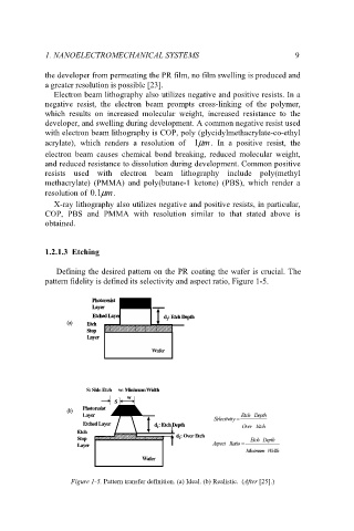
1.2.1.3 Etching
Defining the desired pattern on the PR coating the wafer is crucial. The
pattern fidelity is defined its selectivity and aspect ratio, Figure 1-5.
Photoresist
Photoresist
Layer
Layer
Etched Layer d 1 : Etch Depth
Etched Layer
d 1 : Etch Depth
(a) Etch
(a)
Etch
Stop
Stop
Layer
Layer
Wafer
Wafer
S: Side Etch w: Minimum Width
w: Minimum Width
S: Side Etch
w w
S S
Photoresist
Photoresist
(b)
(b)
Layer Etch DepthEtch Depth
Layer
S
Selectivityelectivit y = =
Etched Layer
Etched Layer d 1 : Etch Depth Over EtchOver Etch
d 1 : Etch Depth
Etch
Etch
d 2 : Over Etch
d 2 : Over Etch
Stop Et Depth
Stop
Etch Depthch
As
Layer
Layer Aspect Ratiopect Ratio = =
Mi
Minimum Widthnimum Width
Wafer
Wafer
Figure 1-5. Pattern transfer definition. (a) Ideal. (b) Realistic. (After [25].)