
Page 27 - Principles and Applications of NanoMEMS Physics
P. 27
1. NANOELECTROMECHANICAL SYSTEMS 13
BrF 3 on the other hand, enables isotropic etching of Si with masking
materials such as Al, Au, Cu, Ni, PR, SiO 2, and Si 3N 4, while achieving
surface finish feature size of 40-150nm. Dry etching, it may be concluded, is
not amenable to creating nanostructures.
1.2.1.4 Chemical Vapor Deposition
The result of patterning a wafer is to render some areas of its surface bare
to receive the deposition of various atomic species, while preventing such
deposition in other areas. Chemical vapor deposition (CVD) is one of the
techniques utilized to introduce atoms into the exposed wafer areas and, for
silicon wafers, entails the dissociation of gasses, such as silane, SiH 4, arsine
(AsH 3), phosphine (PH 3), and diborane (B 2H 6), on the wafer surface at high
temperatures, usually in the 450-800°C range. The chamber containing the
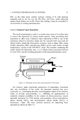
wafers during the deposition, Fig. 1-9, is usually held at pressures between
0.1 and 1Torr, and the resulting properties of the deposited materials varies.
Pressure
Pressure
Sensor Wafers
Wafers
Sensor
3-Zone Furnace
3-Zone Furnace
Pum
Pump p
Load
Load
Door
Door
Gas
Gas
Inlet
Inlet
Figure 1-9. Schematic of hot-wall, reduced pressure CVD reactor.
For instance, under appropriate parameters of temperature, deposition
rate, and crystallinity of the wafer, the deposited material may grow
epitaxially, i.e., maintaining the same crystallographic nature of the substrate
wafer, or become polycrystalline, i.e., exhibiting an agglomeration of
randomly oriented crystallites. In the context of silicon processes, typical
materials deposited via CVD include: polycrystalline silicon (polysilicon),
silicon dioxide (SiO 2), and stoichiometric silicon nitride (Si xN y), to
m
2
thicknesses ~ µ . The most common reactions for depositing these
materials are shown in Table 1-3.