Page 32 - Principles and Applications of NanoMEMS Physics
P. 32

18                                                       Chapter 1


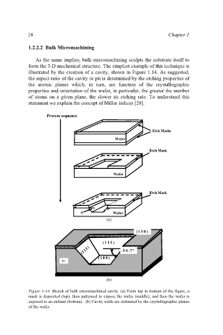
             1.2.2.2 Bulk Micromachining

                As the name implies, bulk micromachining sculpts the substrate itself to
             form the 3-D mechanical structure. The simplest example of this technique is
             illustrated by the creation of a cavity, shown in Figure 1.14. As suggested,
             the aspect ratio of the cavity or pit is determined by the etching properties of
             the  atomic  planes  which, in turn,  are function of the crystallographic
             properties and orientation of the wafer, in particular, the greater the number
             of  atoms  on  a  given plane, the slower its etching rate. To understand this
             statement we explain the concept of Miller indices [28].

                    Process sequence
                    Process sequence

                                                               Etch Masks
                                                               Etch Masks
                                                Wafer
                                                Wafer
                                                              Etch Mask
                                                              Etch Mask


                                               Wafer
                                               Wafer

                                                              Etch Mask
                                                              Etch Mask


                                  θ θ          Wafer
                                               Wafer
                                            (a)

                                                        (110)
                                                        (110)
                                           (111)
                                           (111)
                                  (111)
                                  (111)            54.7  o o
                                                   54.7
                                         (1 00)
                                         (1 00)
                          Si
                          Si
                                            (b)

             Figure 1-14. Sketch of bulk micromachined cavity. (a) From top to bottom of the figure, a
             mask is deposited (top), then patterned to expose the wafer (middle), and then the wafer is
             exposed to an etchant (bottom).  (b) Cavity walls are delimited by the crystallographic planes
             of the wafer.
   27   28   29   30   31   32   33   34   35   36   37