
Page 37 - Principles and Applications of NanoMEMS Physics
P. 37
1. NANOELECTROMECHANICAL SYSTEMS 23
Ele c t r o n - G u n n
Ele c t r o n - G u
E le c tr o n -G u n n
E le c tr o n -G u
Sh ut t e r r
Sh ut t e
(a ) )
( b
(a ( b ) )
Figure 1-20. Electron-beam patterns. (a) Raster scan. (b) Vector scan.
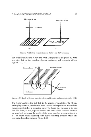
The ultimate resolution of electron-beam lithography is not posed by beam
spot size, but by the so-called electron scattering and proximity effects,
Figures 1-21, 1-22.
Direction of Scan n
Direction of Sca
Electron Beam m
Electron Bea
Desired Line
Desired Line
Resist
Resist
Real Resist
Real Resist
Im age e
Im ag
Substrate te
Substra
Figure 1-21. Sketch of electron scattering effects on PR-coated wafer substrate. (After [23].)
The former captures the fact that, in the course of penetrating the PR and
underlying substrate, the electron beam scatters and experiences a directional
change manifested as a spreading out of the beam, i.e., increase in its spot
size. The latter, in turn, captures the fact that some of the scattered electrons
are absorbed, not under the profile of the beam spot, but in areas adjacent to
it. Two more effects resulting from beam scattering produce width- and
proximity-dependent patterns, Figure 1-22.