
Page 41 - Principles and Applications of NanoMEMS Physics
P. 41
1. NANOELECTROMECHANICAL SYSTEMS 27
the stamp’s recesses. Then, upon curing the polymer, this solidifies
according to the stamp’s pattern. The feature size for patterns thus created
may be as small as 10 nm [34].
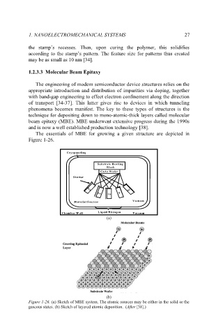
1.2.3.3 Molecular Beam Epitaxy
The engineering of modern semiconductor device structures relies on the
appropriate introduction and distribution of impurities via doping, together
with band-gap engineering to effect electron confinement along the direction
of transport [34-37]. This latter gives rise to devices in which tunneling
phenomena becomes manifest. The key to these types of structures is the
technique for depositing down to mono-atomic-thick layers called molecular
beam epitaxy (MBE). MBE underwent extensive progress during the 1990s
and is now a well established production technology [38].
The essentials of MBE for growing a given structure are depicted in
Figure 1-26.
C ryopanelin
C ryopaneling g
Substrate H eatin
Substrate H eating g
Bloc
Block k
GaAs W afe
GaAs W afer r
Shutte
Shutter r
Al Al
G
Ga a
A P P
A s s
In
In
V acuum
V acuum
M aterial Source
M aterial Sources s
L iquid N itrogen n
Vacuum m
Cham ber W a
Cham ber W all ll L iquid N itroge Vacuu
(a)
(b)
Figure 1-26. (a) Sketch of MBE system. The atomic sources may be either in the solid or the
gaseous states. (b) Sketch of layered atomic deposition. (After [38].)