Page 39 - Principles and Applications of NanoMEMS Physics
P. 39

1. NANOELECTROMECHANICAL SYSTEMS                               25

                                       D
                                       I
                                          R
                                          P
                                    I
                                   L L IQ U ID  P R E CUR S O R T O  P D M S S
                                      U
                                    Q
                                           E
                                                       P
                                                    O
                                                        M
                                                       D
                                                S
                                            CUR
                                                  R T
                                                O
                         MASTER
                                          (a)
                                    M
                                  PD M S  STAMP
                                    M


                PHOTO RES IST

                        (b)                                                                                   (c)
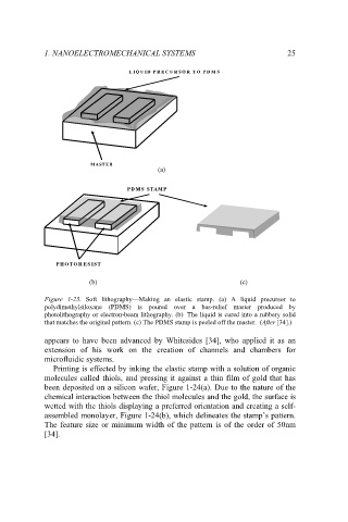
             Figure  1-23. Soft  lithography—Making an elastic stamp.  (a) A  liquid  precursor to
             polydimethylsiloxane  (PDMS)  is poured  over a  bas-relief master produced  by
             photolithography or electron-beam lithography. (b) The liquid is cured into a rubbery solid
             that matches the original pattern. (c) The PDMS stamp is peeled off the master.  (After [34].)
                                                                     (
                                                                     (
             appears to  have  been advanced  by Whitesides [34], who applied  it as an
             extension  of his  work  on the  creation  of  channels and  chambers for
             microfluidic systems.
               Printing is effected by inking the elastic stamp with a solution of organic
             molecules called thiols, and pressing it against a thin film of gold that has
             been deposited on a silicon wafer, Figure 1-24(a). Due to the nature of the
             chemical interaction between the thiol molecules and the gold, the surface is
             wetted with the thiols displaying a preferred orientation and creating a self-
             assembled monolayer, Figure 1-24(b), which delineates the stamp’s pattern.
             The feature size or minimum width of the pattern is of the order of 50nm
             [34].
   34   35   36   37   38   39   40   41   42   43   44