
Page 43 - Principles and Applications of NanoMEMS Physics
P. 43
1. NANOELECTROMECHANICAL SYSTEMS 29
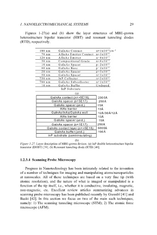
Figures 1-27(a) and (b) show the layer structures of MBE-grown
heterostructure bipolar transistor (HBT) and resonant tunneling diodes
(RTD), respectively.
19
19
m
=1x
1 100 nm G a I n A s C o n t a c t n=1x10 cm -3 -3
G aInA s C o ntact
0
n
n
10
cm
0
19
0
n
m
7 70 nm A l In A s E m i t t e r C o nt a c t n= 1 x1 0 0 19
=
1
x1
n
A lInA s E m itter C o ntact
17
10
0
A lInA s E m itter
m
n
=8x
1
2
120 nm A l I n A s E m i t t e r n n=8x10 17
17
on
o
i
10
t
m
3 30 nm C o m positional G rade e n n=8x10 17
C
G
l
r
a
=8x
a
d
p
m
o
i
0
n
s
18
p= 2x1 0
nm
G aInA s Spacer
10 nm G a I n A s S pac e r p= 2 x 1 0 18
1
0
19
p=
G aInA s B ase
x
6 60 nm G a I n A s B a s e p= 2x1 0 0 19
nm
1
2
0
17
nm
G aInA s Spacer
p= 5x1 0
0
2
20 nm G a I n A s S pac e r p= 5 x 1 0 17
17
m
0
10
n
=1x
G aInA s Spacer
5 50 nm G a I n A s S p a c e r n n=1x10 17
16
l
10
e
or
n
t
c
=3x
0
n
n
5
7 750 nm InP C ollector n=3x10 16
I
P
o
C
l
m
19
0
7
m
=1x
n
0
700 nm G a I n A s S u b c ol l e c t o r n=1x10 19
n
G aInA s S ubcollector
10
10
G aInA s B uffer
10 nm G a I n A s B u f f e r U n do pe d
m
n
U ndoped
InP S ubstrate
In P S u b s t ra t e
(a)
G aInAs contact (n+=5E18) 200 0Å
GaInAs spacer (n=5E17) 250 Å
GaInAs spacer (un d.) 15Å
AlAs barrier 13Å
GaInAs/InAs/G aInA s we ll 12Å/30 Å/12 Å
AlAs barrier 13Å
GaInAs spacer (un d.) 15Å
GaInAs spacer (n=1E17) 250Å
G aInAs contact laye r (n+=5E 18) 500 0Å
G aInAs bu ffe r (und .) 100 Å
InP sub strate (semi-insu lating)
(b)
Figure 1-27. Layer description of MBE-grown devices. (a) InP double heterostructure bipolar
transistor (DHBT) [39]. (b) Resonant tunneling diode (RTD) [40].
1.2.3.4 Scanning Probe Microscopy
Progress in Nanotechnology has been intimately related to the invention
of a number of techniques for imaging and manipulating atoms/nanoparticles
at nanoscales. All of these techniques are based on a very fine tip (with
atomic resolution), and the nature of what is imaged or manipulated is a
function of the tip itself, i.e., whether it is conductive, insulating, magnetic,
non-magnetic, etc. Excellent review articles summarizing advances in
scanning probe microscopy has been published recently by Giessibl [41] and
Baski [42]. In this section we focus on two of the main such techniques,
namely: 1) The scanning tunneling microscope (STM); 2) The atomic force
microscope (AFM).