
Page 38 - Principles and Applications of NanoMEMS Physics
P. 38
24 Chapter 1
B B
C C
A A
Inte
Inter r
Proxim ity
Proxim ity
Intr
Intra a
Proxim ity
Proxim ity
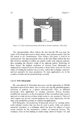
Figure 1-22. Intra- and inter-proximity effects due to electron scattering. (After [23].)
The intra-proximity effect reflects the fact that the PR area near the
center of the beam spot receives more energy, from adjacent points, than the
PR nearest to the circumference. Thus corners, like point A, tend to be
underexposed. The inter-proximity effect, on the other hand, reflects the fact
that electrons intended to define one pattern scatter unto adjacent patterns,
thus extending the effective width of the adjacent pattern. Reflecting all
these factors, the highest resolution of electron beam lithography as
employed for nanoscale device fabrication is about 10nm, however, the slow
nature of writing the patterns one at a time, makes this technique expensive
and not amenable for mass production. Its main applications are in the
creation of masks and in nanotechnology research.
1.2.3.2 Soft Lithography
The conventional IC fabrication processes, and the approaches to MEMS
fabrication derived from them, have as their core step the photolithographic
definition of patterns on a planar substrate/wafer. Thus, as indicated
previously, their application to creating nanoscale devices becomes
prohibitively expensive, as the development of the concomitant light sources
and tools to create devices at these length scales is very expensive. This is of
chief import, not just for research purposes but, more importantly, for the
large scale production germane to commercial applications.
Soft lithography, the production of nanoscale devices by creating elastic
(soft) polymer masters that can then be used to print, mold, and emboss
nanoscale structures, is a technique which has been the subject of much
recent research for the inexpensive creation of nanoscale devices. The
technique relies on first making an elastic stamp, shown in Figure 1-23, and