Page 36 - Principles and Applications of NanoMEMS Physics
P. 36

22                                                      Chapter 1


             1.2.3  Nanoetechnology Fabrication Elements

               The  elements  of nanotechnology fabrication range from techniques to
             produce two-dimensional  patterns with deep-submicron/nanometer-scale
             widths, to techniques to produce atomic-thick layers/multi-layers of various
             material  compositions,  to  techniques  to precisely manipulate atomic-size
             particles.  These techniques,  together  with those presented previously,
             constitute the arsenal at the core of NanoMEMS.


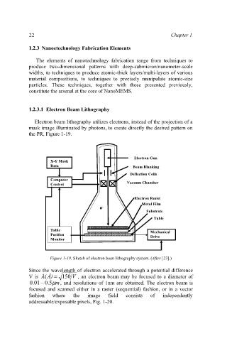
             1.2.3.1 Electron Beam Lithography

               Electron beam lithography utilizes electrons, instead of the projection of a
             mask image illuminated by photons, to create directly the desired pattern on
             the PR, Figure 1-19.


                                                       Electron Gun
                                                       Electron Gun
                     X-Y Mask
                     X-Y Mask
                     Data                             Beam Blanking
                     Data
                                                      Beam Blanking
                                                     Deflection Coils
                                                     Deflection Coils
                     Computer
                     Computer
                                                    Vacuum Chamber
                                                    Vacuum Chamber
                     Control
                     Control
                                                       Electron Resist
                                                       Electron Resist
                                                          Metal Film
                                                          Metal Film
                                         e e - -
                                                            Substrate
                                                            Substrate
                                                               Table
                                                               Table
                     Table
                     Table
                                                             Mechanical
                                                             Mechanical
                     Position
                     Position
                                                             Drive
                                                             Drive
                     Monitor
                     Monitor
                     Figure 1-19. Sketch of electron bean lithography system. (After [23].)
             Since the wavelength of electron accelerated through a potential difference
             V is  (λ Å) =  150  V , an electron beam may be focused to a diameter of
              . 0  01−  5 . 0  µ m, and resolutions of 1nm are obtained. The electron beam is
             focused  and  scanned either  in  a raster (sequential) fashion,  or in a vector
             fashion  where   the   image   field  consists  of   independently
             addressable/exposable pixels, Fig. 1-20.
   31   32   33   34   35   36   37   38   39   40   41