
Page 35 - Principles and Applications of NanoMEMS Physics
P. 35
1. NANOELECTROMECHANICAL SYSTEMS 21
tenths of microns, is stopped after the maximum tolerated lateral etch is
produced. By repeating the passivation/etch sequence, trenches with overall
s
depths of up to several hundred of microns have been demonstrated. The
process proceeds at room temperature, can produce selectivities of 200:1 in
standard PR masks, 300:1 in hard masks such as SiO 2 and Si 3 N 4 , and
exhibits etching rates of 6µ m / sec [30]. As a result of this process, the
walls of the etched trenches exhibit a scalloping structure, see Figure 1-
17(b). The application of DRIE requires acquiring the DRIE equipment. An
alternative to DRIE for better than conventional bulk micromachining, but
not as expensive as DRIE, is presented next.
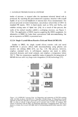
1.2.2.4 Single Crystal Silicon Reactive Etch and Metal (SCREAM)
Similar to DRIE, the single crystal silicon reactive etch and metal
(SCREAM I) process effects bulk micromachining using plasma and
reactive ion etching (RIE) [33], see Fig. 1.18. The process, however,
employs standard tools, is self-aligned, employs one mask to define
structural elements and metal contacts, and employs a temperature below
300 °C. This low temperature capability makes it amenable for integration of
MEMS devices with very large scale integration (VLSI) technology [33].
(a) (e)
(b)
(f)
(c)
(g)
(d)
Figure 1-18. SCREAM I process flow. (a) Deposition and patterning of PECVD masking
oxide. (b) RIE of silicon with BCl 3 /Cl 2 . Typically 4-20 µ m deep. (c) Deposition of oxide
sidewall via PECVD, typically 0.3 µ m thick. (d) Vertical etch of bottom oxide with CF 4 /O 2
RIE. (e) Etch of silicon 3-5 µ m beyond end of sidewall with Cl 2 RIE. (f) Isotropic RIE
release of structures with SF 6 RIE. (g) Sputtering deposition of aluminum metal. The device
shown is a beam, free to move left-right, and its corresponding parallel-plate capacitor. (After
[33].)