
Page 30 - Principles and Applications of NanoMEMS Physics
P. 30
16 Chapter 1
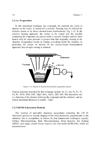
1.2.1.6 Evaporation
In this deposition technique, the evaporant, the material one wants to
deposit on the wafer, is heated off a crucible. Heating may be effected by
resistive means or by direct electron-beam bombardment, Fig. 1-12. In the
resistive heating approach, the wafers to be coated and the crucible
containing the evaporant, are placed inside a vacuum chamber and the latter
heated until its vapor pressure is greater than that originally existing in the
chamber. Evaporation results in coating everything inside the chamber, in
particular, the wafers of interest. In the electron-beam bombardment
approach, line-of-sight coating is obtained.
Substrate
Substrate
B B
Vacuum e BEAM
Vacuum
e BEAM
-+
-+
Evaporant
Evaporant
Figure 1-12. Sketch of electron-beam-based evaporation system.
Typical materials deposited by this technique include Al, Cr, Au, Ni, Fe, Ti,
Cu, Pt, FeNi, TiNi, SiW, MgO, SiO 2, Al 2O 3, AlN, SiN. The deposition rate
is a function of the distance between the evaporant and the substrate, and its
5
m
typical maximum thickness is usually ~ µ .
1.2.2 MEMS Fabrication Methods
The creation of moveable structures necessitates extending the 2-D IC
fabrication process to include shaping of the third dimension, perpendicular to the
substrate; this is exemplified, in silicon, by four fundamental techniques, namely,
Surface Micromachining, Bulk Micromachining, Deep Reactive Ion Etching
(DRIE), and single crystal silicon reactive etch and metal (SCREAM), which are
presented next.