
Page 34 - Principles and Applications of NanoMEMS Physics
P. 34
20 Chapter 1
used for this purpose. However, to accommodate the possibility that the
plane might be parallel to one of the coordinate axes, in which case the
intersection would occur at infinity, the reciprocals of these points of
intersection, (1/h, 1/l, 1/k), are used instead. Figure 1-16(b) shows examples
crystallographic planes and their corresponding of Miller indices [28] for a
cubic crystal such as silicon.
The fact that the aspect ratio of bulk micromachined structures is limited
by the natural inclination of the crystallographic planes making up the walls,
motivated the development of techniques to increase it. The sections below
o
address two f these.
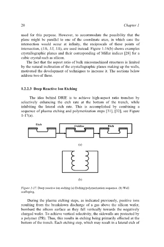
1.2.2.3 Deep Reactive Ion Etching
The idea behind DRIE is to achieve high-aspect ratio trenches by
selectively enhancing the etch rate at the bottom of the trench, while
inhibiting the lateral etch rate. This is accomplished by combining a
sequence of plasma etching and polymerization steps [31], [32], see Figure
1-17(a).
Etch
Etch
Oxidize Etch
Etch
Oxidize
(a)
(b)
Figure 1-17. Deep reactive ion etching (a) Etching/polymerization sequence. (b) Wall
scalloping.
During the plasma etching steps, as indicated previously, positive ions
resulting from the breakdown discharge of a gas above the silicon wafer,
bombard the silicon surface as they fall vertically towards the negatively
charged wafer. To achieve vertical selectivity, the sidewalls are protected by
a polymer (PR). Thus, this results in etching being primarily effected at the
bottom of the trench. Each etching step, which may result in a lateral etch of