Page 19 - Principles and Applications of NanoMEMS Physics
P. 19

1. NANOELECTROMECHANICAL SYSTEMS                                5


             solvent-free dry  layer.  The resulting  PR film thickness is inversely
             proportional  to the square root  of the rotational  speed, and  directly
             proportional to the percent of solids in it. Determining these parameters is
             one of the first steps in developing a process.


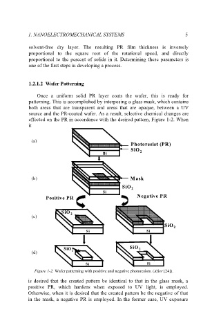
             1.2.1.2 Wafer Patterning

                 Once a uniform solid PR layer coats  the  wafer,  this  is  ready  for
             patterning. This is accomplished by interposing a glass mask, which contains
             both  areas  that are transparent  and areas that  are opaque, between a UV
             source and the PR-coated wafer. As a result, selective chemical changes are
             effected on the PR in accordance with the desired pattern, Figure 1-2. When
             it


              (a)
              (a)
                                                       Photoresist (PR
                                                       Photoresist (PR) )
                                                       SiO  2 2
                                                       SiO
                                           Si
                                           Si
                                                       Mask
              (b)                                     Mask
              (b)
                                                   SiO 2 2
                                                   SiO
                                           Si Si
                                                         Negative PR
                                                         Negative PR
                    Positive PR
                    Positive PR
                          SiO
                          SiO 2 2
              (c)
              (c)
                                                                     SiO
                                                                     SiO
                                                                        2 2
                                    Si Si                    Si Si
                                                      SiO
                           SiO
                           SiO                        SiO 2 2
              (d)
              (d)              2 2
                                    Si Si                    Si Si
               Figure 1-2. Wafer patterning with positive and negative photoresists. (After [24]).
             is  desired  that  the  created  pattern  be identical to that in the glass mask, a
             positive PR,  which hardens when exposed  to  UV  light,  is  employed.
             Otherwise, when it is desired that the created pattern be the negative of that
             in the mask, a negative PR is employed. In the former case, UV exposure
   14   15   16   17   18   19   20   21   22   23   24