
Page 21 - Principles and Applications of NanoMEMS Physics
P. 21
1. NANOELECTROMECHANICAL SYSTEMS 7
centimeters away from the underlying wafer. Because, the contact and
proximity approaches are prone to suffer from dust particles present between
the mask and the PR, the projection approach is preferred for creating
nanoscale-feature patterns. The resolution of a good projection optical
lithography system is given by .0 5 (λ NA ), where λ is the exposure
wavelength and NA is the numerical aperture of the projection optics, at a
depth of focus capability of λ± ( 2 NA ) [23]. The highest resolution of
2
optical photolithography appears to be about 250nm-100nm for production
devices, down to 70nm for laboratory devices, and is set by diffraction, i.e.,
at smaller sizes features become blurred. Overcoming these technical issues,
which involves developing smaller wavelength light sources and optics, is
difficult. Thus, the cost of optical lithography production equipment capable
of reaching resolutions below 100 nm, is deemed by industry as prohibitive
[24].
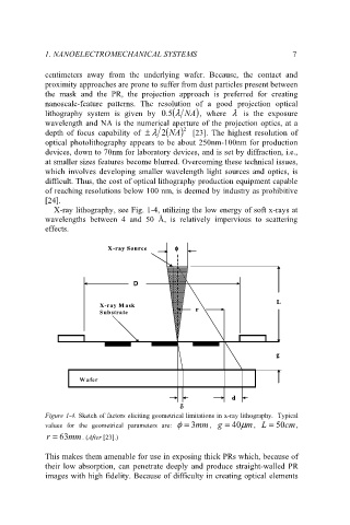
X-ray lithography, see Fig. 1-4, utilizing the low energy of soft x-rays at
wavelengths between 4 and 50 Å, is relatively impervious to scattering
effects.
X -ray Source
X -ray Source φ φ
D D
L L
X-ray M ask
X-ray M ask
r r
Substrate
Substrate
g g
W afer
W afer
d d
δ δ
Figure 1-4. Sketch of factors eliciting geometrical limitations in x-ray lithography. Typical
values for the geometrical parameters are: φ = 3 mm , g = 40 µ m , L = 50 cm ,
r = 63 mm . (After [23].)
This makes them amenable for use in exposing thick PRs which, because of
their low absorption, can penetrate deeply and produce straight-walled PR
images with high fidelity. Because of difficulty in creating optical elements