
Page 141 - Radar Technology Encyclopedia
P. 141
device, negative-resistance device, surface-acoustic-wave (SAW) 131
A negative-resistance device is a microwave device having Relativistic devices can perform amplifier and oscillator
the falling portion of voltage-ampere curve (AB in Fig. D35) functions. IAM
which is characterized by the negative resistance to an alter- Ref.: Kuraev (1986), p. 169.
nating current. The availability of such a characteristic makes
A semiconductor device is based on the use of semiconduc-
possible the generation of continuous waves. The typical
tor properties. The basic types of microwave semiconductor
example of negative-resistance device is the tunnel diode.
devices can be divided into nonjunction (Gunn-effect
SAL
devices), single-junction devices (diodes), and two-junction
Ref.: Leonov (1988), p. 50; Fink (1975), p. 16.43.
(bipolar transistors). Field-effect transistors can be single-
gate or double-gate (field-effect tetrode). Compared with
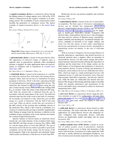
Current Current
electron tubes, semiconductor devices have vital advantages:
A
low mass and size, absence of filament energy expenditures,
higher reliability and operating life, mechanical strength, effi-
Voltage B Voltage ciency, capability of operation at low supply voltages, and
lower cost. For this reason, in most radars semiconductor
devices are used primarily in receiver circuits, and partially in
(a) (b)
transmitting circuits (or entirely, in the case of solid-state
radars).
Figure D35 Voltage-ampere characteristic of (a) conventional
and (b) tunnel diodes (after Leonov, 1988, Fig. 2.15, p. 52). With an increase in frequency, the increasing influence of
parasitic inductances, capacitances and inertial processes in
A piezoelectronic device is based on the piezoelectric effect electrical junctions have a negative effect on operation of
(the appearance of electrical charges of opposite signs at semiconductor devices. For this reason, design and techno-
opposite ends of piezoelectric materials when mechanical logical measures directed towards reducing the capacitance of
pressure is applied). In radar applications these are used pri- junctions and the transit-time of the charge carriers are the
marily in oscillators and as transducers in acoustic-wave chief features of development and production of microwave
delay lines. IAM semiconductor devices. In terms of design and technology of
production, semiconductor devices are subdivided into mono-
Ref.: Fink (1982), p. 13.71; Zherebtsov (1989), p. 164.
lithic, which are made in a single technological process with
A relativistic device is based on the interaction of a rectilin-
integrated circuits of solid-state instruments (most often gal-
ear relativistic electron flow at the input with rotating electro-
lium-arsenide, field-effect transistors), and discrete (individ-
magnetic fields. Such devices have no mechanism for phase
ual), while the latter are subdivided into housed and non-
grouping of electrons, which is the basic operating principle
housed. The design of the housing and leads makes it possible
of conventional power microwave vacuum-tube devices. The
obtain low parasitic inductances and capacitances of the
relativistic flux formed in the gyrotron enters along the axis
devices and makes them convenient to connect to microwave
into a round circular-sweep cavity in which the rotating field
transmission lines. IAM
E 110 is excited. Under the action of the transverse RF mag- Ref.: Fink (1982), p. 6.83; Gassanov (1988), p. 71; Zherebtsov (1989), p. 11.
netic field, the electron flux is deflected from the axis in
accordance with the transit phase of the cavity. The deflected A slow-wave device is a microwave device using the slow-
electrons enter the slot of the cavity in the form of a rectangu- wave structure as a part of its configuration. All main tubes
lar waveguide convoluted in a ring, where they give up their such as the backward-wave tube, klystron, magnetron, travel-
energy as a result of interaction with the field of the main ing-wave tube, and some others are related to slow-wave
wave type. There are device circuits that use conversion of devices. SAL
the drift velocity of the electrons into oscillating velocity of Ref.: Currie (1987), p. 448.
the relativistic flux, which is first swept in a modulator, in a A solid-state device is a microwave device based on solid-
section of a monotonously growing or periodic magnetostatic state technology. The main solid-state devices used in radar
field. Pickup of energy from the electrons is effected on the applications are semiconductor devices and integrated cir-
condition of gyro-resonance in the cavity and does not require cuits. Compared with vacuum-tube devices, solid-state
the creation of high field intensities. devices are significantly smaller and lighter and use much
Specific features of devices based on relativistic fluxes less power. SAL
include the very high intensity of the excitation field (more
Ref.: Kraus (1980); Leonov (1988), p. 51; Tarter (1985).
than 300 kW), the high currents of electron flux (200 to 1000
A surface-acoustic-wave (SAW) device is based on excita-
A), and the output power of more than 600 kW. The type of
tion of surface acoustic waves in piezoelectric materials,
interaction used in the devices makes it possible to practically
propagation of these waves in them, and interaction of the
completely convert the kinetic energy into the energy of the
waves with electrons. Conversion of a radio signal into SAW
electromagnetic field in the decimeter and centimeter bands,
and back is usually effected by interdigital transducers, two
which assures an efficiency of the devices of more than 90%.
rows of interleaved electrodes deposited on the surface of the