Page 309 - Rashid, Power Electronics Handbook
P. 309

15  Resonant and Soft-Switching Converters                                                          299

                 15.14.4 Quasi-Resonant Soft-Switched Inverter                300            V
                          [47]                                                                 cr1
                                                                              200
                 15.14.4.1 Circuit Operation
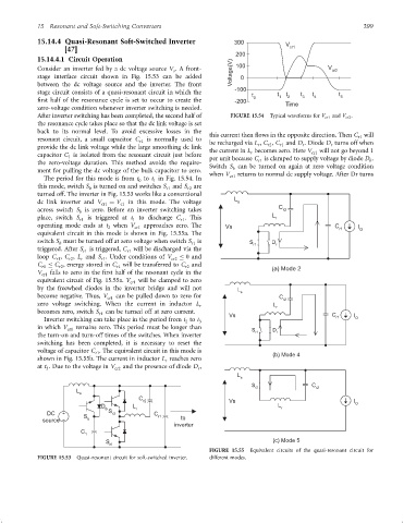
                 Consider an inverter fed by a dc voltage source V . A front-  Voltage(V)  100            V cr2
                                                           s
                 stage interface circuit shown in Fig. 15.53 can be added       0
                 between the dc voltage source and the inverter. The front
                                                                              -100
                 stage circuit consists of a quasi-resonant circuit in which the
                                                                                   t       t 1  t 2  t 3  t 4  t 5
                 ®rst half of the resonance cycle is set to occur to create the  -200  0
                 zero-voltage condition whenever inverter switching is needed.               Time
                 After inverter switching has been completed, the second half of  FIGURE 15.54  Typical waveforms for V cr1 and V cr2 .
                 the resonance cycle takes place so that the dc link voltage is set
                 back to its normal level. To avoid excessive losses in the
                                                                      this current then ¯ows in the opposite direction. Then C will
                                                                                                                   r1
                 resonant circuit, a small capacitor C  is normally used to
                                                 r1                   be recharged via L , C , C and D . Diode D turns off when
                 provide the dc link voltage while the large smoothing dc link       r  r2  r1    r        r
                                                                      the current in L becomes zero. Here V cr1  will not go beyond 1
                                                                                   r
                 capacitor C is isolated from the resonant circuit just before
                           1                                          per unit because C is clamped to supply voltage by diode D .
                 the zero-voltage duration. This method avoids the require-          r1                                b
                                                                      Switch S can be turned on again at zero voltage condition
                                                                             b
                 ment for pulling the dc voltage of the bulk capacitor to zero.
                                                                      when V cr1  returns to normal dc supply voltage. After Dr turns
                   The period for this mode is from t to t in Fig. 15.54. In
                                                     1
                                                0
                 this mode, switch S is turned on and switches S and S are
                                                               r2
                                 b
                                                         r1
                 turned off. The inverter in Fig. 15.53 works like a conventional
                                                                              L
                 dc link inverter and V cr1  ¼ V c1  in this mode. The voltage  s
                 across switch S is zero. Before an inverter switching takes               C r2
                              b
                 place, switch S r1  is triggered at t to discharge C . This             L r
                                                             r1
                                               1
                 operating mode ends at t when V cr1  approaches zero. The  Vs                              C r1    I O
                                       2
                 equivalent circuit in this mode is shown in Fig. 15.55a. The
                 switch S must be turned off at zero voltage when switch S is     S r1   D r
                        b
                                                                 r1
                 triggered. After S r1  is triggered, C r1  will be discharged via the
                 loop C , C , L and S . Under conditions of V cr2    0 and
                               r
                       r1
                                     r1
                           r2
                 C   C , energy stored in C will be transferred to C r2  and             (a) Mode 2
                                          r1
                   r1
                        r2
                 V cr1  falls to zero in the ®rst half of the resonant cycle in the
                 equivalent circuit of Fig. 15.55a. V cr1  will be clamped to zero
                 by the freewheel diodes in the inverter bridge and will not   L s
                 become negative. Thus, V  can be pulled down to zero for
                                       cr1                                                 C r2
                 zero voltage switching. When the current in inductor L
                                                                   r                      L r
                 becomes zero, switch S  can be turned off at zero current.
                                    r1                                      Vs                              C     I
                   Inverter switching can take place in the period from t to t                               r1    O
                                                               2   3
                 in which V  remains zero. This period must be longer than
                           cr1                                                     S     D
                 the turn-on and turn-off times of the switches. When inverter      r1     r
                 switching has been completed, it is necessary to reset the
                 voltage of capacitor C . The equivalent circuit in this mode is         (b) Mode 4
                                   r1
                 shown in Fig. 15.55b. The current in inductor L reaches zero
                                                         r
                 at t . Due to the voltage in V cr2  and the presence of diode D ,
                                                                  r
                    3
                                                                               L
                                                                                s
                                                                                   S r2              C r2
                             L
                              s
                                                C
                                                  r2                        Vs                                    I O
                                     D b       L r                                         L r
                    DC          S      S r2          C r1
                   source        b                           to
                                                           inverter
                               C
                                1
                                      S                                                  (c) Mode 5
                                        r1
                                                                      FIGURE 15.55  Equivalent circuits of the quasi-resonant circuit for
                 FIGURE 15.53  Quasi-resonant circuit for soft-switched inverter.  different modes.
   304   305   306   307   308   309   310   311   312   313   314