Page 308 - Rashid, Power Electronics Handbook
P. 308

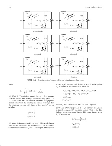
298                                                                                  S. Hui and H. Chung


                                   L                                       L
                                    dc                                      dc
                                                        D2                                     D2
                                           T2                                      T2
                                     T1                  C                  T1                   C
                            Vdc                                  I  Vdc                                 I
                                                  L      r       O                        L      r       O
                                                   r                                       r
                                     C dc                                   C dc
                                            D1                                     D1
                                                   T3                                      T3
                                          (a) normal mode                           (b) mode 1


                                   L                                       L
                                    dc                                      dc
                                                        D2                                     D2
                                           T2                                      T2
                                     T1                  C                  T1                   C
                            Vdc                                  I  Vdc                                 I
                                                  L      r       O                        L      r       O
                                                   r                                       r
                                     C                                      C
                                      dc                                     dc
                                           D1                                      D1
                                                   T3                                      T3
                                            (c) mode 2                              (d) mode 3


                                   L                                       L
                                    dc                                      dc
                                                        D2                                     D2
                                           T2                                      T2
                                     T1                  C                  T1                   C
                            Vdc                                  I  Vdc                                 I
                                                  L      r       O                        L      r       O
                                                   r                                       r
                                     C                                      C
                                      dc                                     dc
                                           D1                                      D1
                                                   T3                                      T3
                                            (e) mode 4                              (f) mode 5
                                    FIGURE 15.52  Operating modes of resonant link inverter with minimum voltage stress.

               where                                                voltage V ðtÞ increases back from 0 to V and is clamped to
                                                                            cr
                                                                                                      s
                                                                    V . The relevant equations in this mode are
                                                                     s
                                s 
                                  L r             1
                            Z ¼       and  o ¼ p                   i ðtÞ¼ ‰I ÿðI on  ÿ I ފ cosðo tÞÿðI on  ÿ I Þ
                                                                            Lr
                                                                                                    r
                                                                                                              s
                                                                                    2
                                                                                             s
                             r
                                            r
                                  C              L C
                                   r               r  r
                                                                           V ðtÞ¼ ‰I ÿðI  ÿ I ފZ sinðo tÞ
                                                                             cr     2   on   s  r    r
               (4) Mode 3 (Freewheeling mode): (t ÿ t )  The resonant      i ðt Þ¼ I
                                                   3
                                               2
               inductor current ¯ows through two freewheeling paths (T2-    Lr 4   3
               Lr-D2 and T3-D1-Lr). This duration is the zero voltage period  V ðt Þ¼ V s
                                                                            cr 4
               created for ZVS of the inverter, and should be longer than
               the minimum on and off times of the inverter's power  where I on  is the load current after the switching state.
               switches:                                            (6) Mode 5 (Discharging mode): (t ÿ t )  In this period, T1 is
                                                                                               4   5
                                                                    switched on under ZV condition because V ðtÞ¼ V . The
                                                                                                          cr     s
                                     i ðtÞ¼ I                       inductor current decreases linearly. This mode ®nishes when
                                     Lr     2
                                                                    i ðtÞ becomes zero.
                                                                     Lr
                                    v ðtÞ¼ 0
                                     cr
                                                                                              V s
                                                                                      i ðtÞ¼ ÿ  t þ I
                                                                                      Lr            3
                                                                                              L
                                                                                               r
               (5) Mode 4 (Resonant mode): (t ÿ t )  This mode begins                 v ðtÞ¼ V s
                                               4
                                           3
                                                                                      cr
               when T2 and T3 are switched off under ZVS. The second half
               of the resonance between L and C starts again. The capacitor          i ðt Þ¼ 0
                                                                                      Lr 5
                                           r
                                     r
   303   304   305   306   307   308   309   310   311   312   313