
Page 307 - Rashid, Power Electronics Handbook
P. 307
15 Resonant and Soft-Switching Converters 297
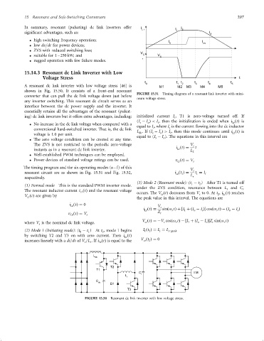
In summary, resonant (pulsating) dc link inverters offer I I
Lr I 1 2
signi®cant advantages, such as: I 3
high switching frequency operation; I I
low dv=dt for power devices; 0 on
ZVS with reduced switching loss;
V
suitable for 1 – 250 kW; and C V S
r
rugged operation with few failure modes.
15.14.3 Resonant dc Link Inverter with Low
Voltage Stress t
t 0 t 1 t 2 t 3 t 4 t 5
A resonant dc link inverter with low voltage stress [46] is M1 M2 M3 M4 M5
shown in Fig. 15.50. It consists of a front-end resonant
converter that can pull the dc link voltage down just before FIGURE 15.51 Timing diagram of a resonant link inverter with mini-
mum voltage stress.
any inverter switching. This resonant dc circuit serves as an
interface between the dc power supply and the inverter. It
essentially retains all the advantages of the resonant (pulsat-
ing) dc link inverters but it offers extra advantages, including: initialized current I , T1 is zero-voltage turned off. If
i
(I ÿ I Þ < I , then the initialization is ended when i ðtÞ is
o
i
Lr
s
No increase in the dc link voltage when compared with a equal to I , where I is the current ¯owing into the dc inductor
conventional hard-switched inverter. That is, the dc link i s
L .If (I ÿ I Þ > I , then this mode continues until i ðtÞ is
s
Lr
dc
i
o
voltage is 1.0 per unit.
equal to (I ÿ I ). The equations in this interval are
o
s
The zero voltage condition can be created at any time.
The ZVS is not restricted to the periodic zero-voltage V s
i ðtÞ¼ t
Lr
instants as in a resonant dc link inverter. L 2
Well-established PWM techniques can be employed.
Power devices of standard voltage ratings can be used. v ðtÞ¼ V
cr s
The timing program and the six operating modes (a – f) of this V
resonant circuit are as shown in Fig. 15.51 and Fig. 15.52, i ðt Þ¼ L s t ¼ I i
Lr 1
1
respectively. r
(3) Mode 2 (Resonant mode): (t ÿ t ) After T1 is turned off
2
1
(1) Normal mode This is the standard PWM inverter mode.
under the ZVS condition, resonance between L and C r
r
The resonant inductor current i ðtÞ and the resonant voltage occurs. The V ðtÞ decreases from V to 0. At t , i ðtÞ reaches
Lr
2
s
cr
V ðtÞ are given by the peak value in this interval. The equations are Lr
cr
i ðtÞ¼ 0
Lr V s
i ðtÞ¼ sinðo tÞþI þðI ÿ I Þ cosðo tÞÿðI ÿ I Þ
s
Lr
o
1
o
s
r
r
v ðtÞ¼ V Z r
Cr s
V ðtÞ¼ÿV cosðo tÞÿ I þðI ÿ I ÞZ sinðo tÞ
where V is the nominal dc link voltage. cr s r 1 o s r r
s
(2) Mode 1 (Initiating mode): (t ÿ t ) At t , mode 1 begins I ðt Þ¼ I ¼ I Lr;peak
L 2
2
0
0
1
by switching T2 and T3 on with zero current. Then i ðtÞ
Lr
increases linearly with a di=dt of V =L .If i ðtÞ is equal to the V ðt Þ¼ 0
cr 2
Lr
r
s
L
dc
T2
T1
C I.M.
L r
r
C
dc
D1
T3
FIGURE 15.50 Resonant dc link inverter with low voltage stress.