Page 306 - Rashid, Power Electronics Handbook
P. 306

296                                                                                  S. Hui and H. Chung

                             R        L                                 Integral pulse-density modulation has to be used. Many
                                                                        well-established PWM techniques cannot be employed.
                                 I L                +
                    V                               V      I        Despite these advantages, this resonant converter concept has
                     S                               C      X       paved the way for other soft-switched converters to develop.
                                                    -
                                      S
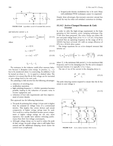
                                                                    15.14.2 Active-Clamped Resonant dc Link
                    FIGURE 15.48  Equivalent circuit of resonant link inverter.
                                                                             Inverter
                                                                    In order to solve the high-voltage requirement in the basic
               and inductor current i is
                                  L
                                                                    pulsating dc link inverters, active clamping techniques (Fig.

                                              V s                   15.49) have been proposed. The active clamp can reduce the
                               ÿat
                    i ðtÞ  I þ e  I cosðotÞþ    sinðotÞ     ð15:15Þ
                     L
                           x
                                   M
                                              oL                    per-unit peak voltage from 2.0 to  1:3ÿ1:5 [41]. It has been
                                                                    reported that an operating frequency in the range of 60 to
               where                                                100 kHz has been achieved [45] with an energy ef®ciency of
                                                                    97% for a 50-kVA drive system.
                                   a ¼ R=2L                 ð15:16Þ   The design equations for an active-clamped resonant link
                                                                    inverter are
                                          ÿ0:5
                                 o ¼ðLCÞ                    ð15:17Þ
                                   o
                                                                                                    p  !
                                                                            1    p           kð2 ÿ kÞ
                                        2   2 0:5                                         ÿ1
                                  o ¼ðo ÿ a Þ               ð15:18Þ    T ¼    ¼ 2 L C r  cos ð1 ÿ kÞþ            ð15:20Þ
                                                                                   r
                                                                        L
                                        o
                                                                            f L                       k ÿ 1
               and
                                                                    where T is the minimum link period, f is the maximum link
                                   I M  ¼ I ÿ I x           ð15:19Þ        L                        L
                                         Lo
                                                                    frequency, and k is the clamping ratio. For the active-clamped
                                                                    resonant inverter, k is typically 1.3 to 1.4 p.u.
                 The resistance in the inductor could affect resonant beha-
                                                                      The rate of rise of the current in the clamping device is
               vior because it dissipates some energy. In practice, (i ÿ I )
                                                            L
                                                                x
               has to be monitored when S is conducting. In addition, S can
               be turned on when (i ÿ I ) is equal to a desired value. The             di   ðk ÿ 1ÞV s
                                     x
                                 L
               objective is to ensure that the dc link voltage can be resonated        dt  ¼  L r                ð15:21Þ
               to zero voltage level in the next cycle.
                 The pulsating dc link inverter has the following advantages:
                                                                    The peak clamping current required to ensure that the dc bus
                    reduction of switching loss;                    return to zero voltage is
                    snubberless operation;
                    high switching frequency (>18 kHz) operation becomes                   s 
                    possible, leading to the reduction of acoustic noise in                  kð2 ÿ kÞC r
                                                                                     I ¼ V s                     ð15:22Þ
                                                                                     sp
                    inverter equipment; and                                                     L r
                    reduction of heat sink requirements and thus improve-
                    ment of power density.
                 This approach has the following limitations:
                                                                           Vcc
                    The peak dc pulsating link voltage (2.0 per unit) is higher
                    than the nominal dc voltage value of a conventional      Lr
                    inverter. This implies that power devices and circuit
                    components of higher voltage ratings must be used.
                    This could be a serious drawback because power compo-
                                                                           Vdc
                    nents of higher voltage ratings are not only more           Cr
                    expensive, but usually have inferior switching perfor-
                    mance than their low-voltage counterparts.
                    Although voltage clamp can be used to reduce the peak
                    dc link voltage, the peak voltage value is still higher than
                    normal and the additional clamping circuit makes the
                    control more complicated.                              FIGURE 15.49  Active-clamp resonant link inverter.
   301   302   303   304   305   306   307   308   309   310   311