
Page 33 - Renewable Energy Devices and System with Simulations in MATLAB and ANSYS
P. 33
20 Renewable Energy Devices and Systems with Simulations in MATLAB and ANSYS ®
®
2.2 PV POWER
PV cells, or solar cells, are semiconductor devices that convert solar energy directly into DC electric
energy. In the 1950s, PV cells were initially used for space applications to power satellites, but in
the 1970s, they began also to be used for terrestrial applications [7, 8]. Today, PV cells are used to
provide power in a wide variety of applications, including grid-connected systems (e.g., utility scale
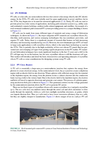
and residential), remote buildings, outdoor traffic-related equipment, and satellites. An example of a
roof-mounted residential grid-connected PV system providing power to a campus building is shown
in Figure 2.2.
PV cells can be made from many different types of materials and using a range of fabrication
techniques. As shown in Figure 2.1, the major categories of PV materials are crystalline silicon (Si),
thin film, multi-junction, and various emerging technologies like dye-sensitized, perovskite, and
organic PV cells. Today, there is a significant amount of research that focuses on both increasing
efficiency and decreasing manufacturing cost [9]. However, the most dominant type of PV cell used
in large-scale applications is still crystalline silicon, which is the same basic technology as used in
the 1970s. This is partially due to the high availability of low-cost silicon PV panels that has pre-
vented new and emerging cell types from gaining significant presence in the PV market. PV materi-
als and fabrication techniques have made significant headway in the last 15 years and a shift in the
PV cell type may be on the horizon, but, for now, crystalline silicon is still the dominant cell type.
This section will introduce and detail the basic characteristics and operating principles of crystalline
silicon PV cells as some considerations for designing systems using PV cells.
2.2.1 PV Cell Basics
A PV cell is essentially a large-area p–n semiconductor junction that captures the energy from
photons to create electrical energy. At the semiconductor level, the p–n junction creates a depletion
region with an electric field in one direction. When a photon with sufficient energy hits the material
in the depletion region, the energy from the photon excites a valance electron into the conduction
band, leaving a hole in the valance band. Due to the electric field in the depletion region, the electron
and hole will travel in opposite directions and generate a net current. This process of a photon gener-
ating an electron–hole pair is shown in Figure 2.3. This generated current over the voltage generated
by the semiconductor junction allows the PV cell to generate DC power.
There are two basic types of crystalline silicon cells: mono-crystalline (m-c) and poly-crystalline
(p-c). The m-c cells have one uniform lattice through the entire cell and allow electronics to flow
easily through the materials, while p-c cells have multiple crystalline structures, or grains, which
can impede electron flow. Thus, p-c cells tend to have lower conversion efficiency than m-c cells,
but they are slightly cheaper to manufacture. Figure 2.4 shows images of an m-c and p-c PV cell
FIGURE 2.2 Roof-mounted grid-connected PV system at Ulsan National Institute of Science and Technology
in Ulsan, South Korea.