
Page 34 - Renewable Energy Devices and System with Simulations in MATLAB and ANSYS
P. 34
Solar Power Sources: PV, Concentrated PV, and Concentrated Solar Power 21
–– ++
–– ++
P N
–– ++
–– ++
E-field
Electron
Photon
E c
E f
Hole
E v
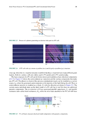
FIGURE 2.3 Process of a photon generating an electron–hole pair in a PV cell.
(a) (b)
FIGURE 2.4 A PV cell with (a) a mono-crystalline (m-c) and (b) poly-crystalline (p-c) structure.
close-up, where the m-c material structure is uniform but the p-c materials have many different grain
regions. Both m-c and p-c cells are widely used in PV panels and in PV systems today.
The basic structure of a PV cell can be broken down and modeled as basic electrical components
[10–12]. Figure 2.5 shows the semiconductor p–n junction and the various components that make
up a PV cell. The photon-to-electron flow process explained previously can be modeled as a current
source, I , where the generated current depends on the intensity of the light hitting the cell. The p–n
ph
semiconductor junction is modeled as a diode, D, with the direction as shown in Figure 2.5. The
current source and diode make up the ideal model of a PV cell, but in real life there are additional
parasitic components. The p–n junction will have associated parallel capacitance, C , and parallel
p
resistance (also called shunt resistance), R , while the wire leads attached to the PV cell will have
sh
(Back)
P C p I pv +
I ph D R sh V pv
N –
(Front) R s L s
Sunlight
FIGURE 2.5 PV cell basic structure electrical model components with parasitic components.